Simple slave camera flash (or synchronous flash, like this one I built earlier) works great with older film cameras, but does not work with modern digital cameras. This is due to the fact that the majority of the digital cameras nowadays employee a so-called pre-flash for metering purposes prior to the actual shooting. The pre-flash causes the slave flash to be triggered prematurely which inter has a detrimental effect on the picture taken, causing the scene to be darker then done without using the slave flash since the camera thinks the environment was lighter than it actually was when the slave flash was triggered.
In order to tackle this pre-flash phenomenon and synchronize the slave flash with the main flash event, we have a couple of obvious options:
- Add some delay to the slave unit so that it fires after the pre-flash when triggered.
- Ignore the pre-flash event and synchronize with the main flash.
The first option is the easiest to implement, but the time delay has to match the interval between the pre-flash and the main flash in order to obtain the optimal result. Unfortunately, this delay timing is somewhat difficult to achieve as the interval may differ among different cameras and under different circumstances. Even for the same camera, the interval could vary as well (for instance, I measured the interval on my Cannon PowerShot ELPH 300 HS. The pre-flash to main flash interval is somewhere between 90 to 110 milliseconds).
This leaves us with the second option — ignore the pre-flash and synchronize the slave unit with the main flash. The obvious advantage of this approach is that we no longer need to know the time delay between the pre-flash and the main flash. But it does make the circuit a bit more complex.
Since the latter option is arguably more versatile, we will use it in our design.
Circuit Design
The following timing diagram illustrates what we are trying to achieve:
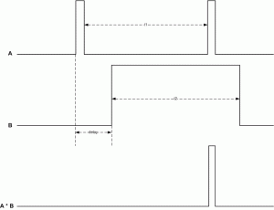
The top waveform shows the timing of the camera flash firing events. The first pulse is the pre-flash and the latter one is the main flash. Our goal is to generate a triggering waveform for the slave flash similar to the last one in the diagram shown above, effectively ignoring the pre-flash.
In order to achieve this, we will need a control waveform similar to the waveform shown in the middle. The control waveform is triggered by the pre-flash and is delayed by some time. The delay time is not critical as long as the pulse’s rising edge occurs prior to the main flash. And the pulse’s width needs to be longer than the main flash’s falling edge so that the during the main flash firing the control pulse remains at high.
If the properties mentioned above for the control pulse are satisfied, we can simply perform an “AND” operation between the detected camera flashes and the control signal and obtain our slave flash triggering signal waveform (C).
Some may be asking, why not just use a counter circuit to control the slave flash? For instance, why not just count the pulses and only trigger the slave flash when the count is two? Well, in principal this approach would also work. But in practice, it has some serious drawbacks. The main problem is that the flash event may not be correctly detected. If this happens, the counter circuit will be out of sync. Of course we can always automatically reset the counter after a brief period, but this would make the circuit more complicated than necessary. Another issue with the counter approach is that we need to know the exact number of pre-flash events. While for the majority of situations we can safely assume that only one pre-flash is fired, but for some cameras there could be occasions in which multiple pre-flashes occur before the main flash is engaged. This would make the counter method difficult to implement. So by using some delay to ignore the pre-flashes, we can easily adjust the delay time as long as we know the approximate timing of when the main flash fires.
The following is the circuit diagram of the camera flash controller I designed. It operates by delaying the triggering signal and synchronizing with the main flash event.
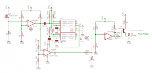
Here is how it works. IC2A forms a comparator circuit with hysteresis, it normally outputs HIGH. When the camera flash is fired, the voltage at the negative input to the comparator will rise above that of the positive input and the comparator will output a low pulse. This output pulse then goes to a 556 timer (two 555’s) which is configured as two chained monostable single-shot circuits. The first stage generates a pulse with a width of 1.1*R7*C3 (roughly 10ms using the values supplied), and at the falling edge of this pulse the second stage is triggered. The second stage has a delay of 1.1*R9*C4 (roughly 500ms). As mentioned earlier, the delay of the first stage needs to be shorter than the time delay before the main flash fires, and the delay of the second stage needs to last longer than the falling edge of the main flash as illustrated in the timing diagram above.
Besides triggering the monostable circuit, the output of IC2A is also passed through an inverted comparator IC2B to output a positive pulse. No hysteresis is necessary for this comparator as the input is from IC2A’s output which is guaranteed to be rail-to-rail (or the maximum and minimum output voltages of the comparator). Finally the output from IC2B, now a positive pulse, along with the output from the second stage of the timer go into IC2C. IC2C is configured as an AND gate. When both of the inputs are high, the input voltage at the positive input of the comparator will become higher than that at the negative input and IC2C will output a high. Because IC2C is an AND gate, the width of the output pulse is the shorter one among the two inputs and in this case the pulse width would be comparable to the pulse generated by the main flash.
LM339’s current output capability is quite limited and thus a transistor is added to provide the required gate current to trigger the SCR (thyristor). Alternatively, IC2C’s output can be used to drive an IGBT directly as I described earlier.
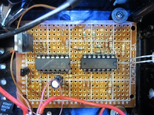
This circuit is fairly easy to build, here is a picture of my finished circuit built on a perfboard.
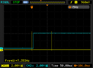
Just to confirm our theory of operation, I took a couple of oscilloscope captures below (single shot, triggered by channel 1):
 |
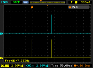 |
In both captures, channel one is probed at test point 1 (TP1 in schematics). Channel two is connected to test point 2 (the output of the second stage of the monostable circuit) in the left image and connected to test point 3 (the output of the AND gate) in the image to the right.
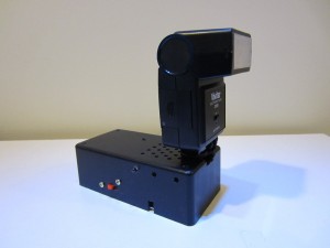
The supply voltage is not critical in this design and you can power the circuit anywhere between 5V to 12V. Since the current requirement is very low, I used a 9V battery. Everything fits pretty nicely in a small project base as you can see in the picture below.
Here are a couple of pictures taken with my Cannon PowerShot ELPH 300 HS with this slave flash. In order for the picture not to be washed out, I had to reduce the intensity of the slave flash.
 |
 |

