One of the biggest advantages of FRAM (or FeRAM, Ferroelectric RAM) over EEPROM is that FRAM has a much higher write speed and typically can operate at bus speed. This means that no delay instructions are needed when performing write operations, which greatly reduces coding complexity and increases the overall throughput. FRAM is also capable of supporting beyond 1012 read/write cycles whereas most EEPROM can only handle around 106 read/write cycles. These properties make FRAM very attractive for using with microcontrollers where frequent write to nonvolatile memory is needed.
In this blog post I will give an example on interfacing two Ramtron FM25C160 FRAM chips with Arduino. Since the basic operations on an FRAM are very similar to those on a standard EEPROM, I would recommend reading this SPI EEPROM tutorial first if you are not familiar with the protocol.
The main difference between the operation modes of an FM25C160 and a standard EEPROM is that FM25C160 allows multi-byte sequential reads and writes whereas EEPROM typically has a limited write buffer and long writes beyond the buffer length must be broken into multiple writes. We will take advantage of this in our code later.
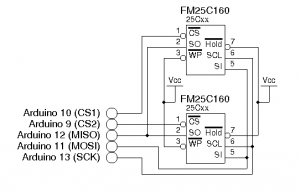
The following schematic shows the simplest way to interface multiple FRAM (or EEPROM) chips with Arduino.

For our simple implementation, the HOLD and WP pins are disabled (tie to Vcc) and the corresponding data pins (SO, SI and SCK) are connected together. The CS pin of each FRAM is controlled individually by an Arduino IO pin so that each FRAM can be selected and operated on individually.
The following code shows how to access multiple FRAM chips using Arduino. For FM25C160, the maximum address is 0x7FF (since it has 16 Kbits and 2K bytes) so we assume that addresses between 0x800 and 0x1000 belong to the second chip, and addresses beyond 0x1000 are invalid.
#include <SPI.h>

const byte CMD_WREN = 0x06; //0000 0110 Set Write Enable Latch
const byte CMD_WRDI = 0x04; //0000 0100 Write Disable
const byte CMD_RDSR = 0x05; //0000 0101 Read Status Register
const byte CMD_WRSR = 0x01; //0000 0001 Write Status Register
const byte CMD_READ = 0x03; //0000 0011 Read Memory Data
const byte CMD_WRITE = 0x02; //0000 0010 Write Memory Data

const int FRAM_CS1 = 10; //chip select 1
const int FRAM_CS2 = 9; //chip select 2

/**
 * Write to FRAM (assuming 2 FM25C160 are used)
 * addr: starting address
 * buf: pointer to data
 * count: data length.
 *        If this parameter is omitted, it is defaulted to one byte.
 * returns: 0 operation is successful
 *          1 address out of range
 */
int FRAMWrite(int addr, byte *buf, int count=1)
{
  int cs = 0;

  if (addr > 0x7ff)  {
    addr -=0x800;
    cs = FRAM_CS2;
  } else {
    cs = FRAM_CS1;
  }

  if (addr > 0x7ff) return -1;

  byte addrMSB = (addr >> 8) & 0xff;
  byte addrLSB = addr & 0xff;

  digitalWrite(cs, LOW);
  SPI.transfer(CMD_WREN);  //write enable
  digitalWrite(cs, HIGH);

  digitalWrite(cs, LOW);
  SPI.transfer(CMD_WRITE); //write command
  SPI.transfer(addrMSB);
  SPI.transfer(addrLSB);

  for (int i = 0;i < count;i++) SPI.transfer(buf[i]);

  digitalWrite(cs, HIGH);

  return 0;
}

/**
 * Read from FRAM (assuming 2 FM25C160 are used)
 * addr: starting address
 * buf: pointer to data
 * count: data length.
 *        If this parameter is omitted, it is defaulted to one byte.
 * returns: 0 operation is successful
 *          1 address out of range
 */
int FRAMRead(int addr, byte *buf, int count=1)
{
  int cs = 0;

  if (addr > 0x7ff)  {
    addr -=0x800;
    cs = FRAM_CS2;
  } else {
    cs = FRAM_CS1;
  }

  if (addr > 0x7ff) return -1;

  byte addrMSB = (addr >> 8) & 0xff;
  byte addrLSB = addr & 0xff;

  digitalWrite(cs, LOW);

  SPI.transfer(CMD_READ);
  SPI.transfer(addrMSB);
  SPI.transfer(addrLSB);

  for (int i=0; i < count; i++) buf[i] = SPI.transfer(0x00);

  digitalWrite(cs, HIGH);

  return 0;
}

void setup()
{
  Serial.begin(9600);
  pinMode(FRAM_CS1, OUTPUT);
  digitalWrite(FRAM_CS1, HIGH);
  pinMode(FRAM_CS2, OUTPUT);
  digitalWrite(FRAM_CS2, HIGH);

  //Setting up the SPI bus
  SPI.begin();
  SPI.setDataMode(SPI_MODE0);
  SPI.setBitOrder(MSBFIRST);
  SPI.setClockDivider(SPI_CLOCK_DIV2);

  //Test
  char buf[]="This is a test";

  FRAMWrite(1, (byte*) buf, 14);
  FRAMRead(1, (byte*) buf, 14);

  for (int i = 0; i < 14; i++) Serial.print(buf[i]);
}

void loop()
{
}
While the above code supports memory spanning multiple chips, each read/write operation is limited within a single chip. This should be sufficient under most scenarios. If reading/writing beyond a single chip’s boundary is required, logic needs to be added so that when the address wraps around to 0 the CS of the current chip is deselected and the CS of the next chip is selected.

