Many of the modern chips such as MEMS accelerometers and gyroscopes only come in surface mount versions and many of them come in fine pitch LGA or QFN packaging. This has created a significant challenge for people who just wanted to experiment with these components. The standard soldering technique for LGA/QFN chips is reflow soldering which requires special equipment such as reflow oven and hot air rework station. Special surface mount prototyping PCBs are also needed and these PCBs, depending on the size and complexity can be quite expensive and sometimes are pricier than the components themselves.
Luckily, most of these LGA and QFN chips can be prototyped on the typical 2.54 mm drill hole spacing protoboard. In this post, I will use STMicroelectronics‘ LPY450AL dual-axis gyroscope IC as an example to show how to hand solder this kind of fine pitch chips on a protoboard. I have used similar techniques extensively in many of my previous projects (1, 2, 3). When done properly, this technique can be used in prototyping most lower pin count LGA/QFN chips. Even some chips in the RF range (such as Si4301) can be prototyped this way.
LPY450AL comes as a tiny LGA-28 chip measuring at just 4x5x1mm. The pad spacing is very small (0.5 mm). But this chip can be soldered using a standard fine-tip soldering iron with some practice and patience.
Chip Placement
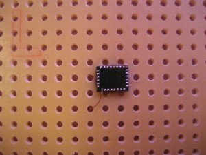
Chip should be placed on the component side of the board with pads facing up. Depending on the external components used for your particular circuit, you will need to decide where on the board the chip should be placed. Since LPY450AL requires only a handful of external components, I put it at the center of a small protoboard (see below).
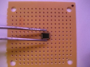
Since the chip is flipped upside down, you will need to pay special attention to the pin numbering. I placed a black mark at the top right corner of the board to indicate the location of pin 1. This chip has a tiny marking near pin 1 as well but not all chips have such identification on the bottom side. Also, the pin ordering would now be clockwise instead of counter clockwise when viewed from the top.
After you are satisfied with the chip placement, use a drop of super glue to glue the chip in place. A pair of tweezers will come in handy for some fine adjustments.
Tinning The Pads
You will need to use a soldering iron with a fine tip. If you have a temperature controlled iron, try setting it to the lowest recommended temperature for the type of solder you are using. For Pb-free solder, this temperature should be around 245 degree Celsius and for Sn-Pb solder, the temperature should be around 215 Celsius. If you do not have a temperature controlled soldering iron, you can use a small wattage one (e.g. 15W-25W) attached to a dimmer switch (note, dimmer switch does not regulate the temperature of the iron. Since the pads and wires we are dealing with are very tiny, the temperature change of the iron tip is quite negligible). You can test the iron tip temperature using a thin piece of solder. The temperature should be adjusted such that it is just adequate to melt the solder. Since the pads on these LGA/QFN chips are very fragile, too high of a temperature can result in the detachment of the pads and essentially ruin the chip. You will be warned on this multiple times later.
The picture below shows the soldering iron I used (no temperature control).
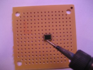
The pads should be tinned first prior to soldering. To tin the pads, first apply some flux on them, and then use the tip of the soldering iron to gently touch each individual pads. Note that the pads on LGA/QFN devices are not designed to withstand excessive force, do not use the tip to drag laterally on the pads as they may come off as a result. Since the surface area of each pad is extremely small, it heats up quickly and usually a pad can be tinned within a second of iron contact.
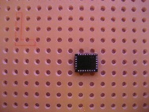
Here is a picture I took after the pads were tinned. Depending on the type of flux you used, you may or may not need to clean up the flux residue.
Soldering
I would highly recommend using the copper wires within the stranded hookup wire for this task. For each pad, a single strand should be used. Thin magnetic wires could be used as well, but you will need to remove the insulation layer carefully prior to soldering to ensure good connectivity.
Wires should first be soldered onto the pads on the chip and then soldered onto the protoboard. Before soldering on to the pad, the tip of the wire should first be tinned. Then, carefully place the tip of the wire onto the pad. Use the tip of the iron to briefly tap the wire from above. With a little bit of pressure, the wire should bound to the already tinned pad. Again, do not rub the pad with the tip of iron to prevent pad from detaching. After removing the soldering iron, wait for a few seconds for the joint to cool and then gently pull the wire to ensure that it is soldered onto the pad.
Then, the other end of the wire can be soldered on to the protoboard. Since the wire is very thin, you do not have to worry about it coming off the soldering pad as a result of soldering it on to the protoboard.
It might be easier to solder all the pads first since it could be a bit more difficult to fix the connections on the pads once the wires are already soldered onto the protoboard. Sometimes the already soldered wire could come off the pad due to the heat generated while soldering on an adjacent pad (use the finest tip you have to avoid this issue). It would be easier to redo the soldering when the other end of the wire is still free.
Try keeping the wires as short as possible to minimize the stray capacitance and inductance, especially when dealing with circuit that runs at higher frequencies.
Again, it is important for the soldering tip not to stay on each pad for too long at any given time. Typically, a couple of seconds should be sufficient to get the job done. If you need to touch up your work, wait till the pads cool down first before trying again. Also, always apply force perpendicular to the pads. All these precautions can greatly reduce the risk of damaging the chip while soldering.
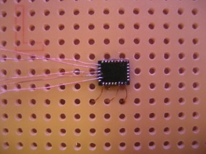
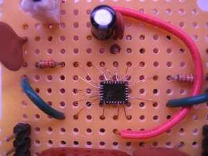
Here is the completed LPY450AL experiment board. You can see how tiny the chip is compared to the rest of the circuit components. To put things in scale, the resistors I used are 1/16 watt.
