Hantek‘s 2D72 (and 2D42) is the latest handheld oscilloscope in the 2000 series that combines an oscilloscope, a multimeter and an arbitrary waveform generator all inside a single device that is not much bigger than a full sized DMM. I did a thorough video review of it a few days ago (see video link below) and was quite impressed at its performance. In this blog post, I will share with you some of the teardown pictures. A video of the teardown is also linked towards the end of the post.
The main difference between the 2D72 and 2D42 models is the oscilloscope bandwidth. The 2D72 model has a bandwidth of 70MHz whereas the 2D42 model has a bandwidth of 40MHz. There are two C models (2C72 and 2C42) as well, they do away with the arbitrary waveform generator and come at a reduced price point. In my opinion though the extra cost for the AWG functionality is definitely worth the money as the arbitrary waveform generator can come in handy in a lot of the situations.
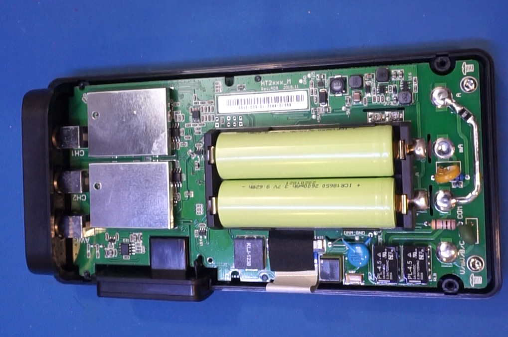
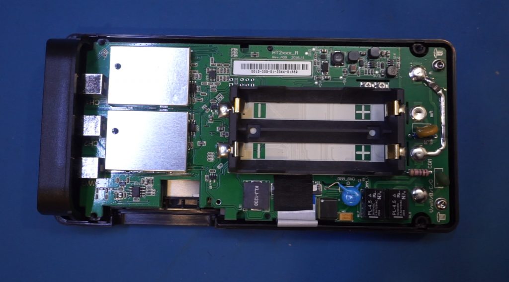
After removing the rubber holster and a couple of screws, the back can be easily removed. The unit is powered by two 18650 Lithium ion batteries. Below is a picture showing the first glance of the internals. Note that if you just need to change the batteries, you can do so via the access panel at the back without having to remove the holster or the back of the case.
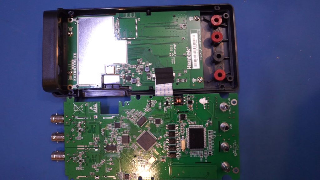
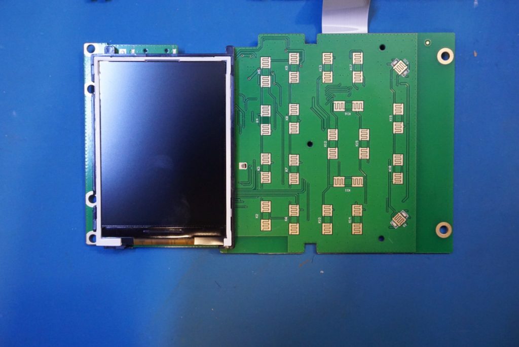
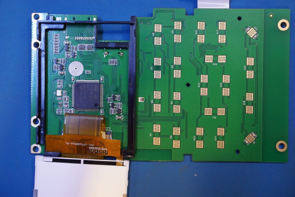
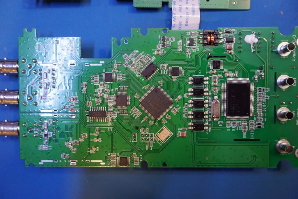
The unit employees a two boards design. One board houses the key logic section that supports the OSC/DMM/AWG, and the other board mainly takes care of the display.
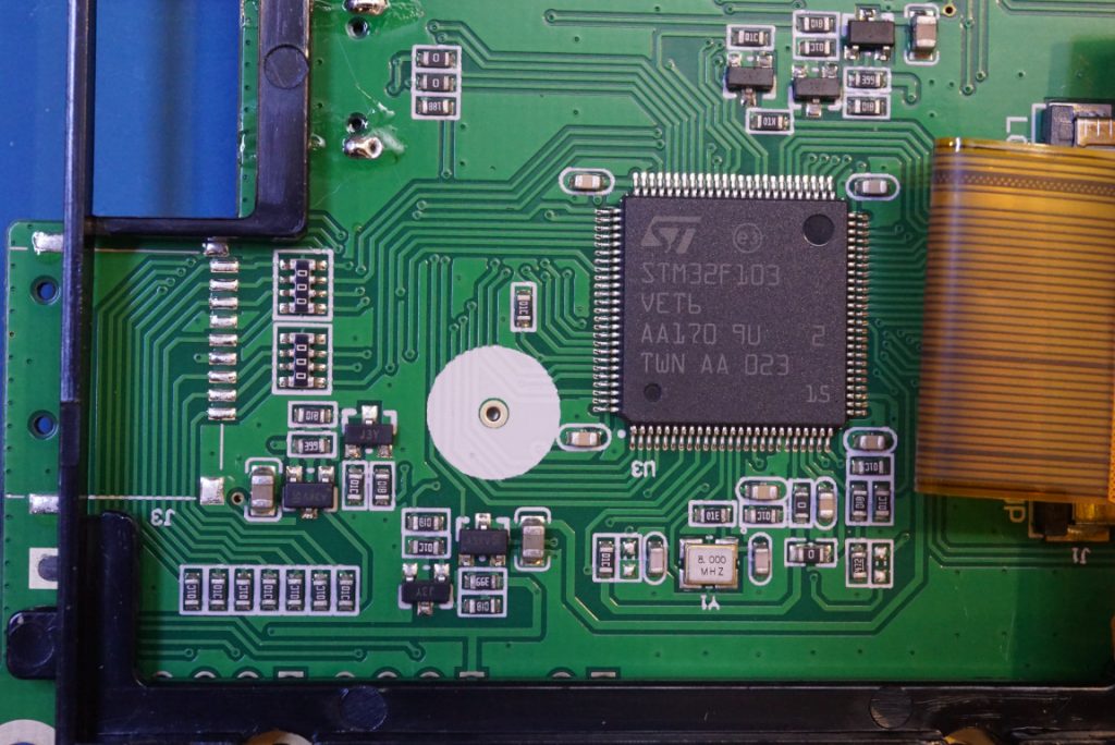
First let’s examine the display board in a bit more details. In the pictures below, you can see the circuitry underneath the LCD. An STM32F103 is used to handle the GUI display and presumably the all the user inputs.
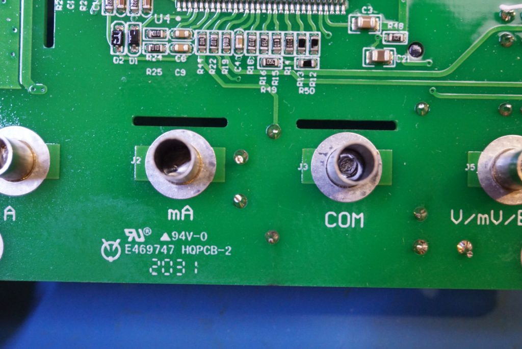
Note the empty foot print (J3) in the image below. The unpopulated footprint is for an SD card reader. Interestingly, the unit also has a matching slot on the case that corresponds to the SD slot. Not sure why the card reader is never implemented in the 2D72 even though it is the top of the line model in the 2000 sereies.
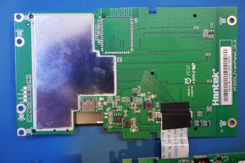
On the reverse side of the display board, you can see a USB connector that is recessed from the edge of the board. I am not entirely sure why the USB connector was deigned not to be flush with the edge of the board as the port is quite recessed making it more difficult to plug in the USB cable.
There is also an empty footprint reserved for an ESP8266 module by the look of it. Again, could it be that Hantek has a future version planned that incorporates both an SD card and a wireless module?
To the left of the board you can see the programming headers for the MCU. The reverse side of the display is shielded. I suspect there are probably only a few passives if any at all underneath the shielding and thus I didn’t bother removing it.
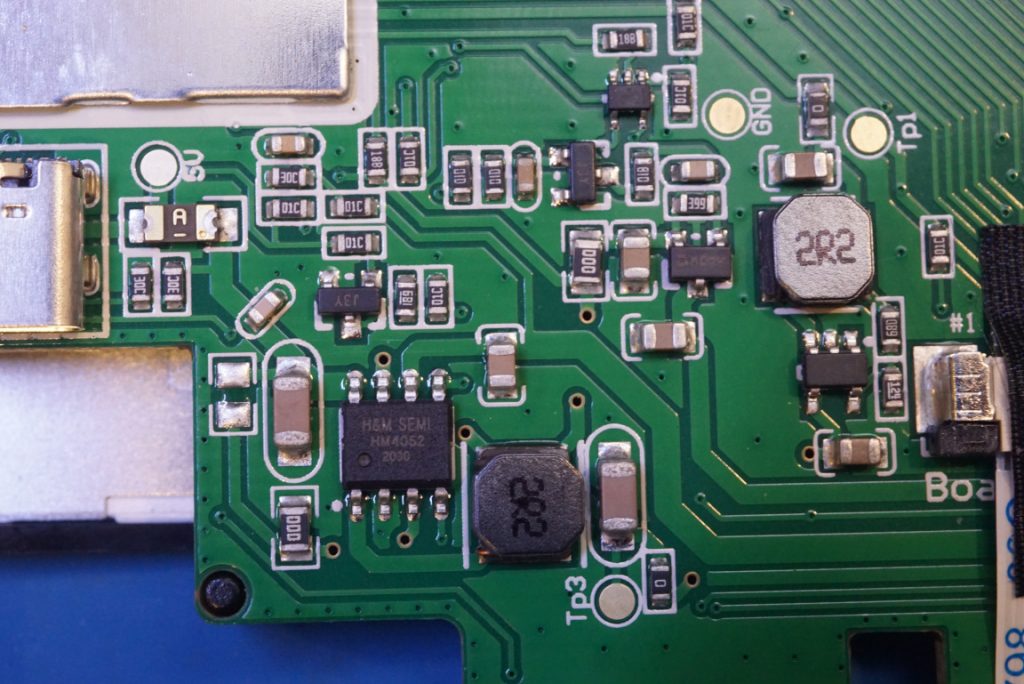
The battery charging circuitry is also implemented on the LCD board. It uses an HM4052 Lithium ion battery charging controller as you can see in the closeup picture below. The two 18650 lithium ion cells are configured in parallel with independent balancing control on the cathode side.
Now moving onto the main logic board. This oscilloscope has two independent input channels.
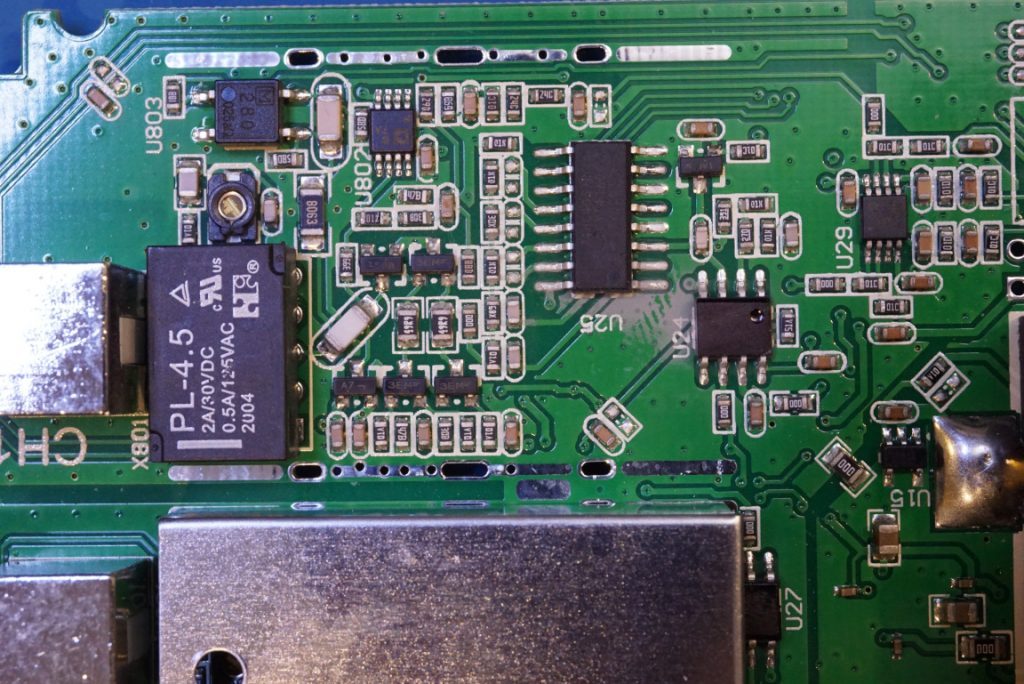
The picture to the left below shows one of the channels after removing the shielding can. The other channel should be identical. There is a single relay for input attenuation switching. In the picture you can also see a frequency response tuning capacitor. The 16 chip (U25) is an CD4051 8 channel MUX.
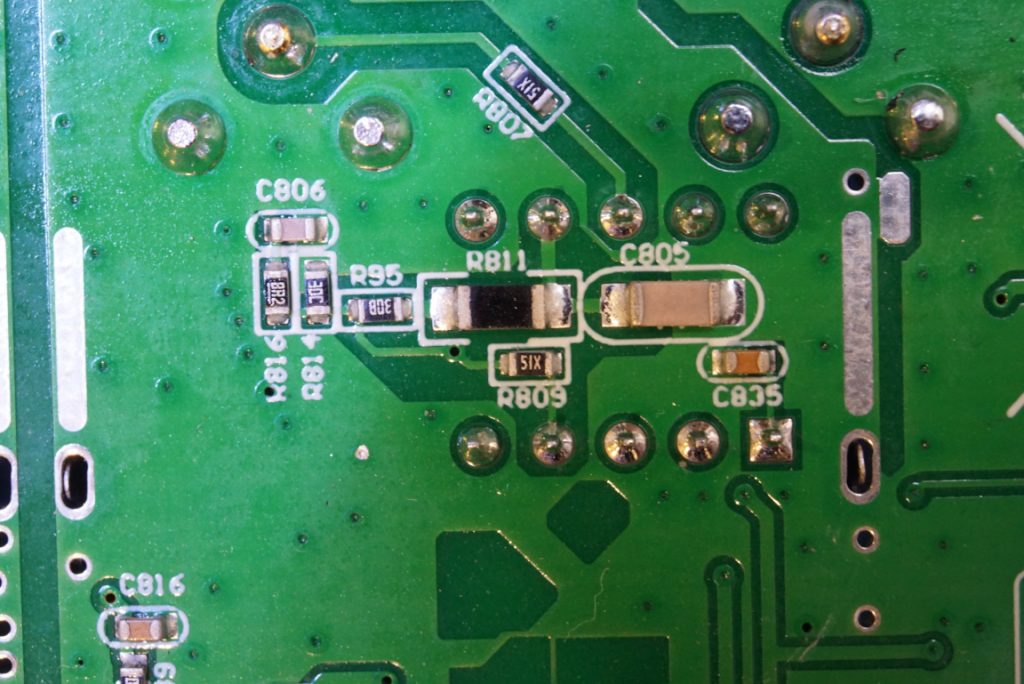
The picture to the right below shows the underside of input channel.
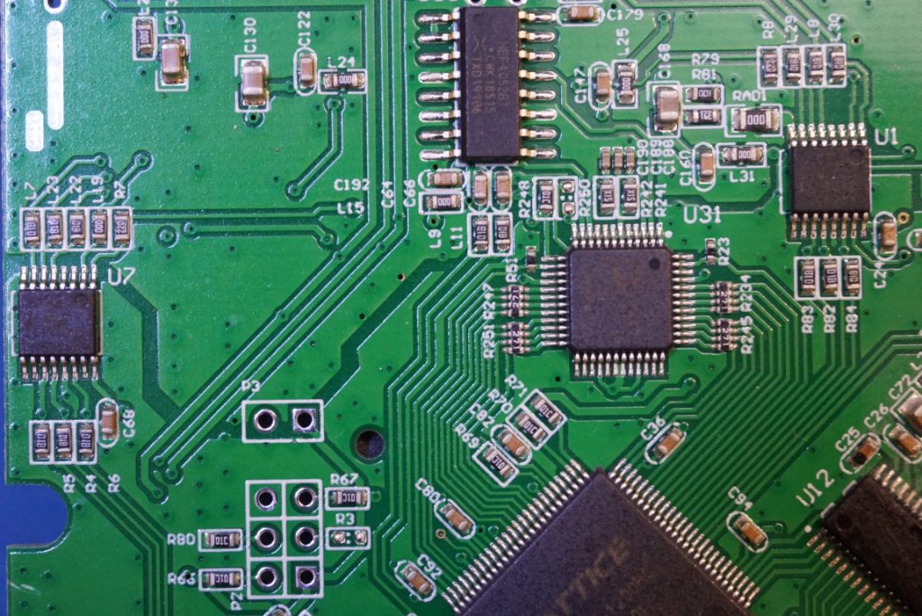
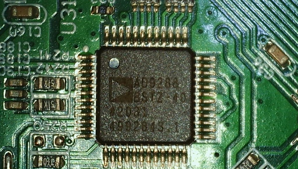
The analog to digital converter used for the front-end is an AD9288 8-bit 100 MSPS dual A/AD converter. It is interesting to note that the maximum sampling rate for a single channel is specified at 250 MSPS, not entirely sure how this is achieved using an 100MSPS ADC.
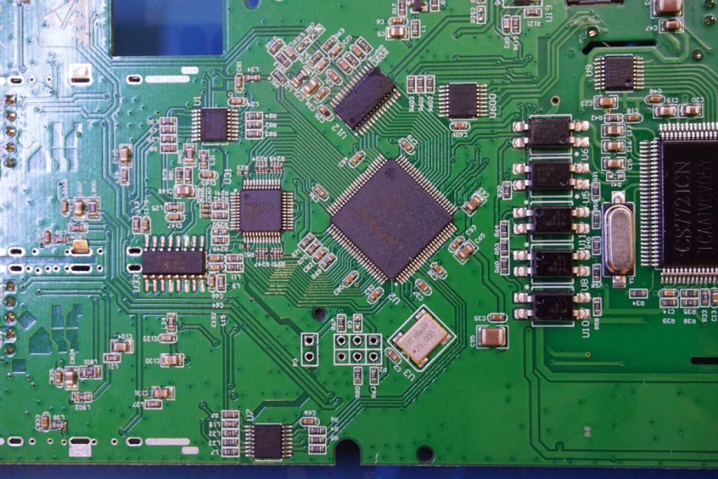
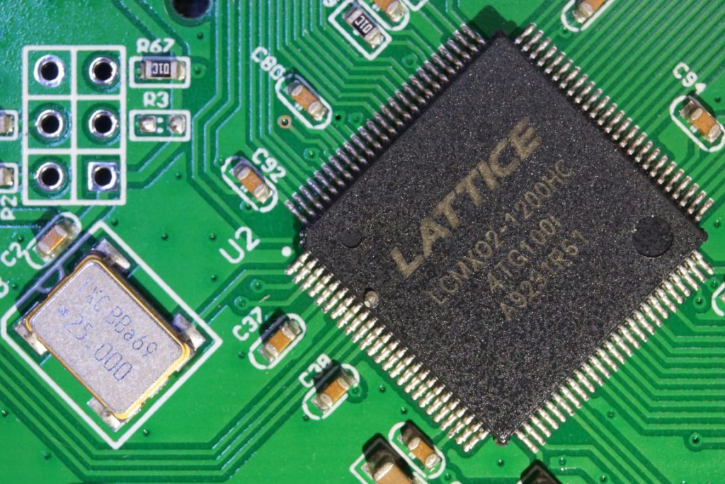
Hardware capability is implemented with a Lattice LCMXO2-1200HC FPGA. If you look at the 28 pin chip towards the top in the picture to the left below you will see that the chip has its markings sanded off. Given that the 2D72 also has the signal generator functionality, this chip is almost certainly a DAC. The pin layout seems to match that of an DAC902, a 12-bit 165 MSPS digital to analog converter.
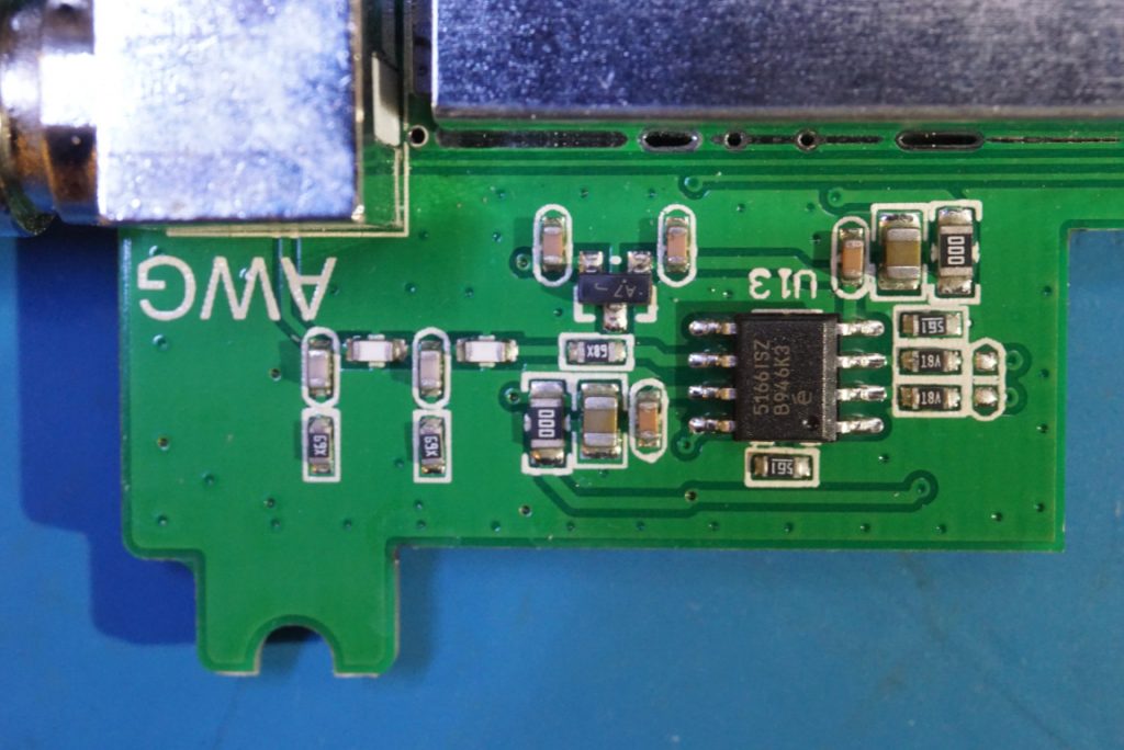
The output from the DAC is routed to the other side of the board and inputs into a Renesas EL5166 current feedback amplifier which drives the output.
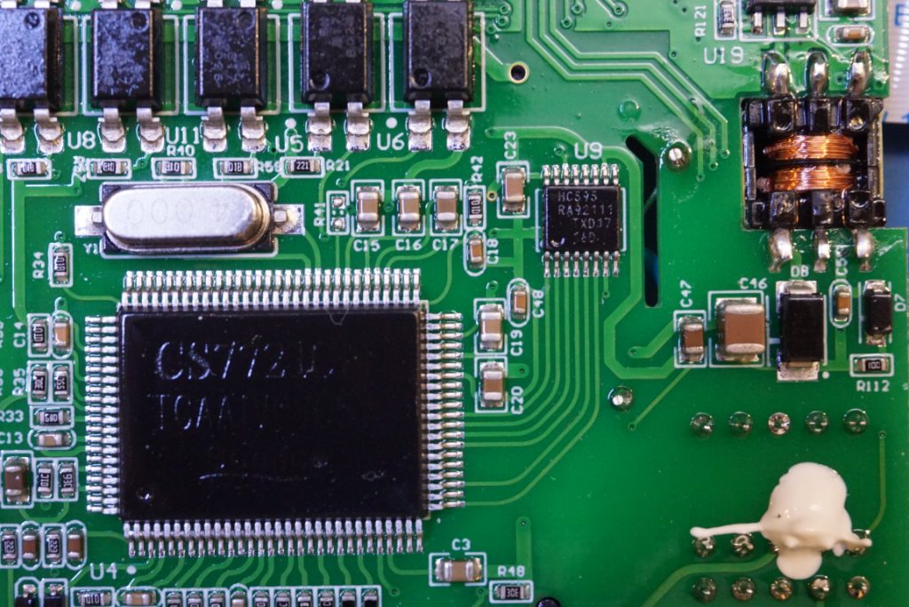
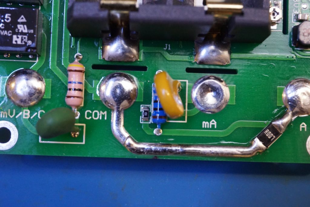
Digital multimeter is implemented using a dedicated DMM chip – a 4000 count CS7721. Note that the bank of optocouplers that isolate the DMM portion from the rest of the circuitry. The input protection is somewhat lacking. There is a single PTC on the voltage input side. In the low current range, there is a polyfuse for over current protection. Due to the space constraints however, there is no fuse in the high current measurement range. Given that the shunt resistor is relatively small, in an over current event the current shunt would most likely fail first and thus almost serves like a fuse. I’d still prefer an appropriately rated fuse in the high current range however. Similar products from Owon’s HDS series do have fused Amp range measurements and offer much more precision (20,000 counts) in the DMM range.
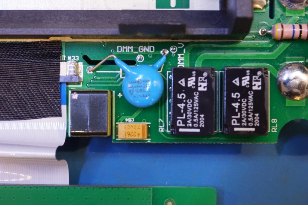
Because there is no physical range switch to speak of, two relays are used to switch the input based on the desired measurement range. You can also see a MOV on the input side that is used to clamp down any transient. Also you will notice quite a few isolation slots in the DMM input section.
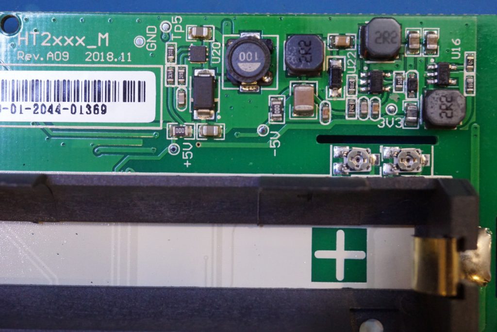
On the other side of the battery holder, you can see some DC/DC converters used to provide all the required power rails. The two trimmer pots in the picture below belongs to the DMM section and are probably used for calibration purpose.
Below is a video of the teardown.
