I did a detailed review of an MSO2304X 300 MHz, quad channel 5 GSa/s mixed signal oscilloscope from UNI-T recently. The MSO2000X series is quite capable. Besides being a 4 channel digital oscilloscope, it also includes a builtin logic analyzer with the optional UT-M15 logic pod. The scope has builtin protocol analyzer and Bode plot analyzer. For more details, please check out my review video linked below. In this blog post, I will share some of the teardown pictures and provide some of my analysis.
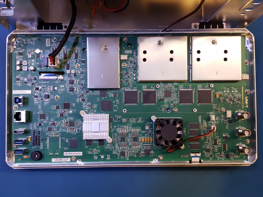
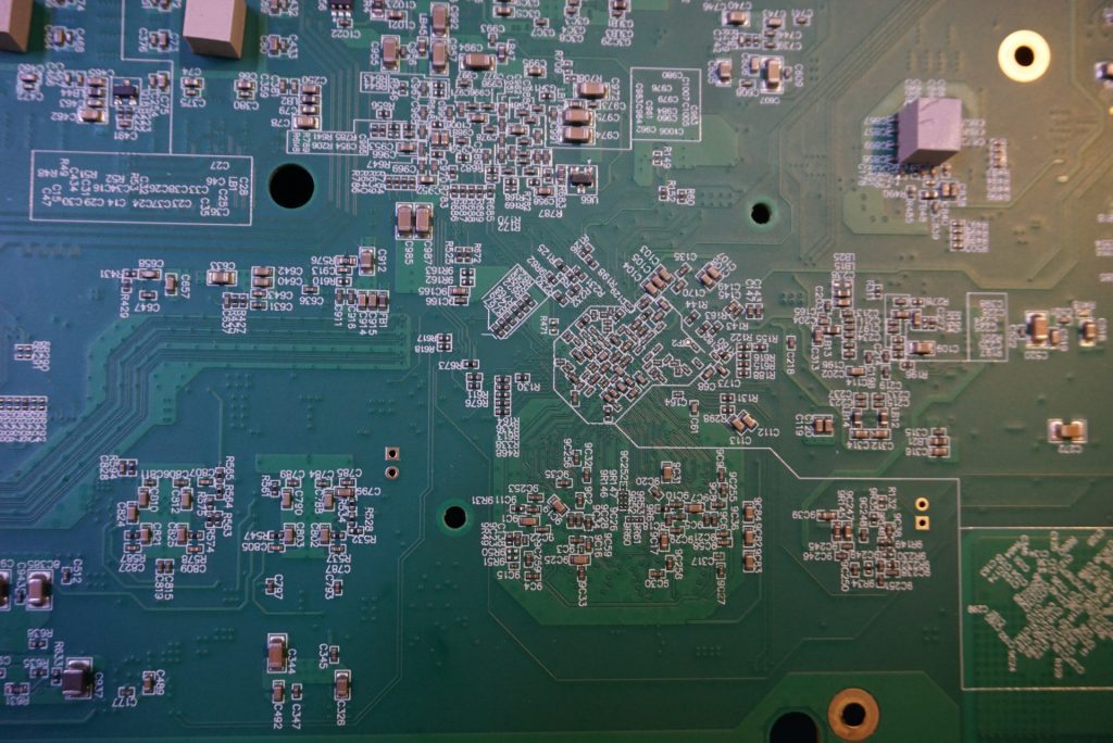
Here is a picture of the main PCB. The input channels and function generator output sections are under the shielding cans.
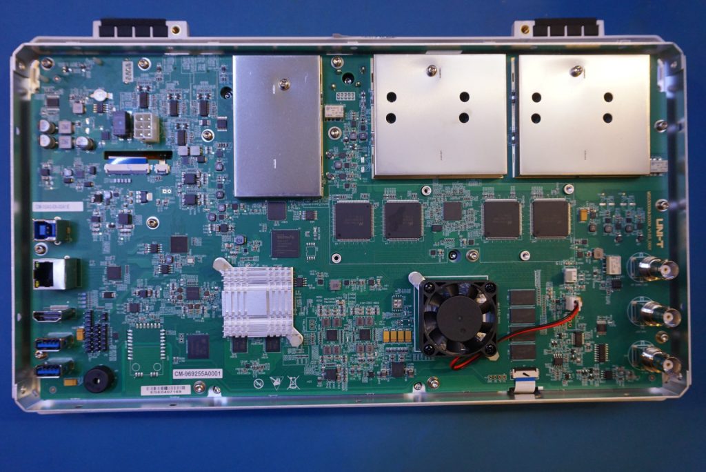
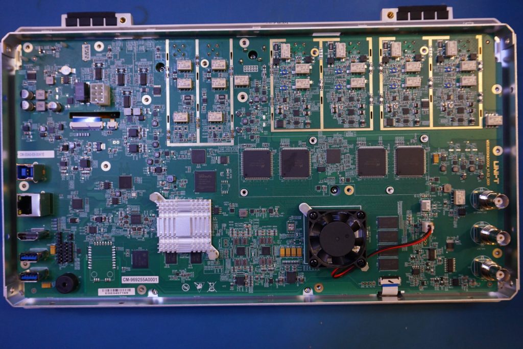
Here are a couple more pictures of the main board, the image to the right has all the shielding cans removed.
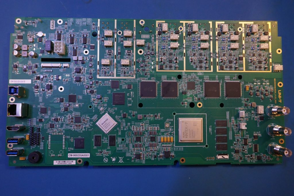
Here is a picture with the heatsinks removed from the main FPGA and application processor.
Here is picture of the signal generator portion of the circuit. There are two independent channels. Each channel has a 49.9 Ω resistor and that is because the signal generator supports both 1 MΩ and 50Ω output impedance.
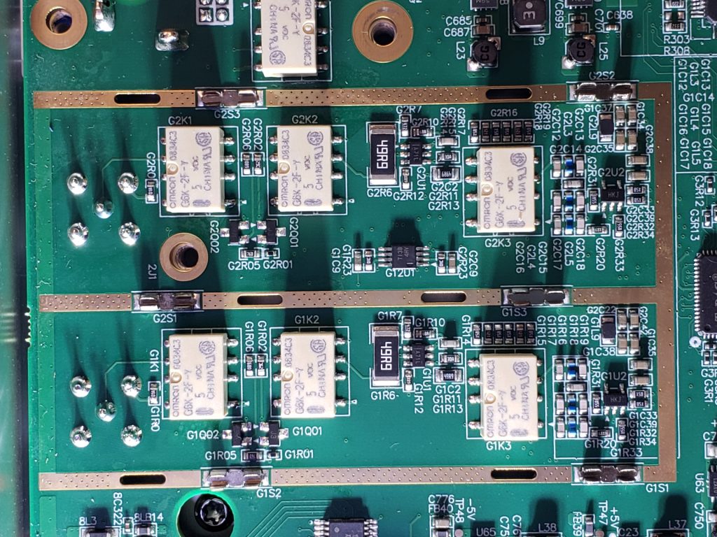
Below is a picture showing the circuitry between the signal generator section and the oscilloscope channel one input section. In the MSO2000X series, the scope probe compensation test signals can be configured to output different frequencies. Each of the test output ports can be configured to output 10 Hz, 100 Hz, 10 kHz and 100 kHz square waves.
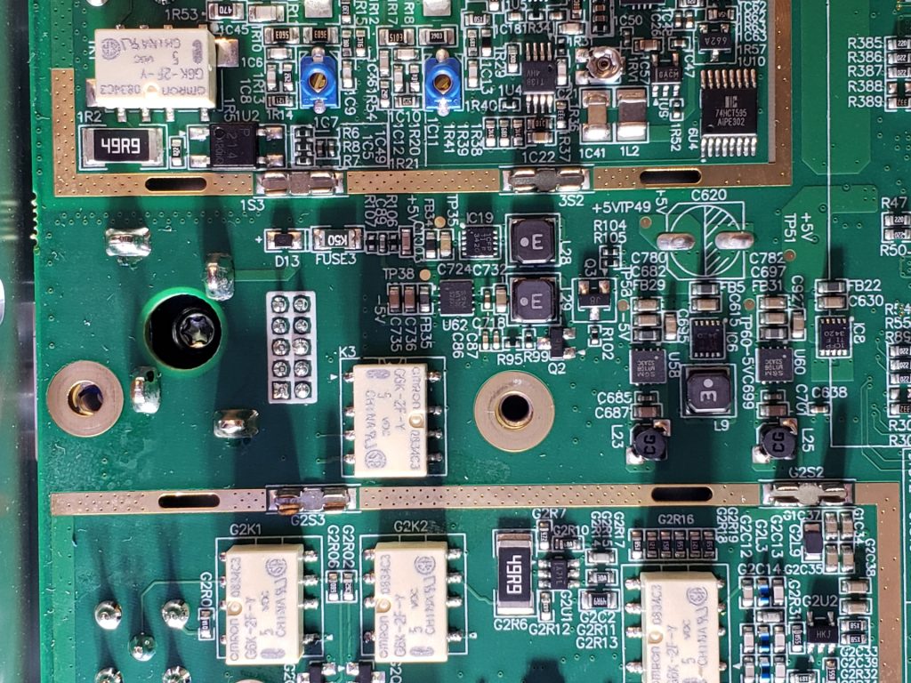
Here are some pictures of the four input channels. The main circuitry for these four input channels are largely identical, except for the 595 shift registers on channel 1 and channel 3. Channel 3 also has a chip marked X78C, it appears to be a octal 12-bit DAC DAC128S085
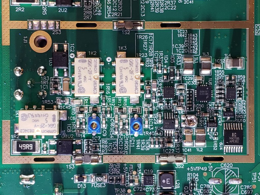
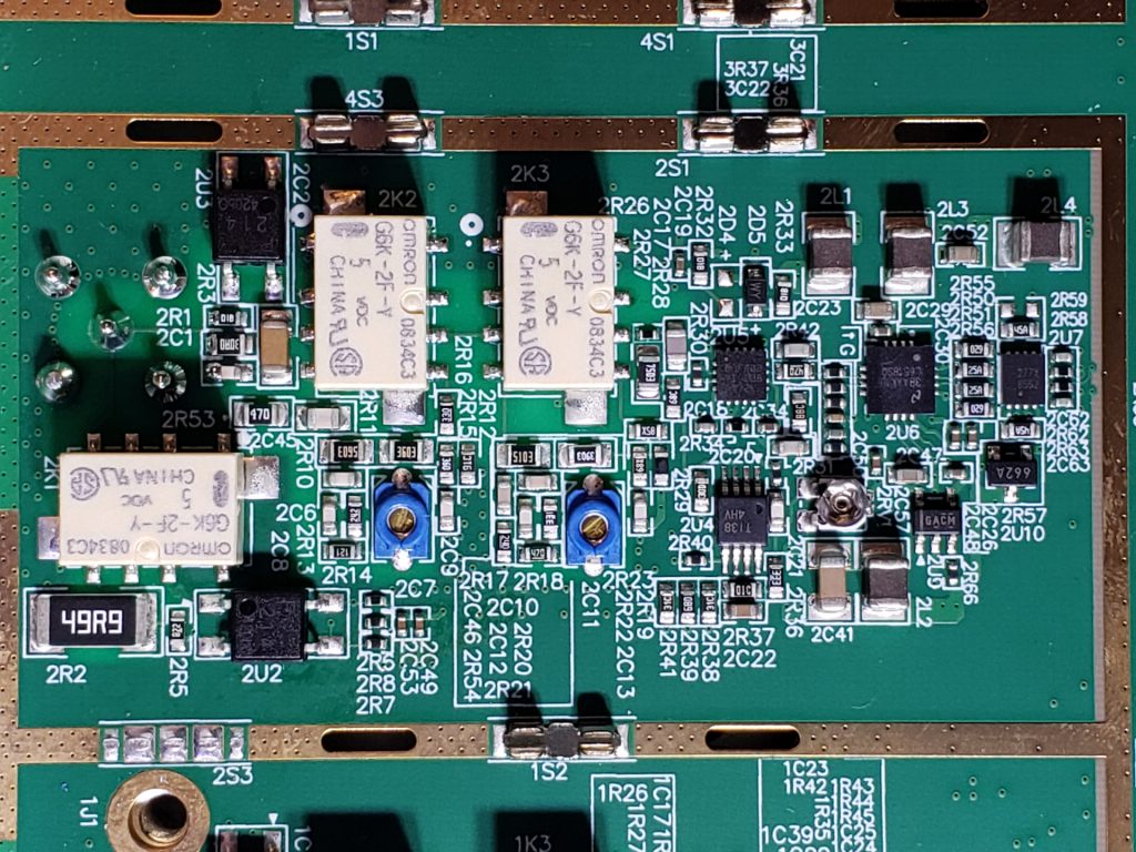
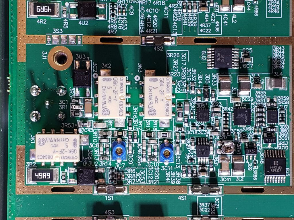
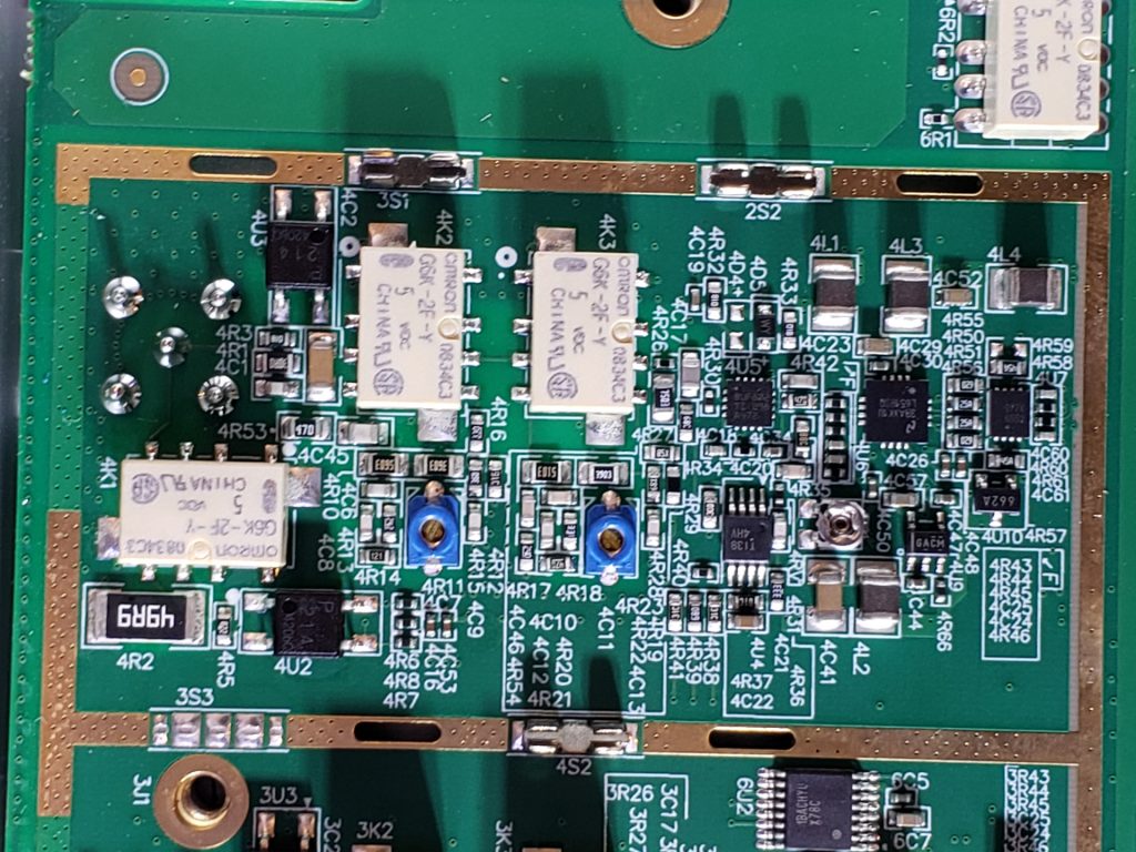
Each channel has a 49.9Ω resistor. Just like the signal generator output channels, the oscilloscope input channels also support either 1MΩ or 50Ω input impedance and can be configured.
To achieve the 300 MHz input bandwidth, UNI-T used a LMH6518 which is a 900 MHz digitally controlled variable gain amplifier, it has very fast rime time of less than 500 ps. There is also a high speed opamp, the BUF802. It has a gain bandwidth of 3.1 GHz.
The trimmer caps are used for calibrate the frequency response. There is also a trimpot in each channel, presumably to fine tune the gains.
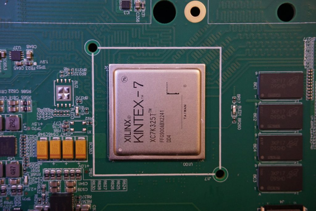
The main application processor and the main FPGA are under the heatsinks. Upon removing the heatsinks, you can see the chips used. For the main application processor, UNI-T used an Rockchip RK3568, it is a quad-core ARM Cortex-A55 processor and is quite capable. The main FPGA used is an Xlinx KINTEX-7 XC7K325T. This is a powerful FPGA, it has 326,080 logic cells.
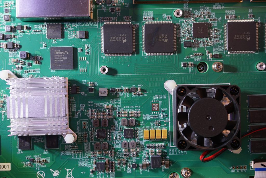
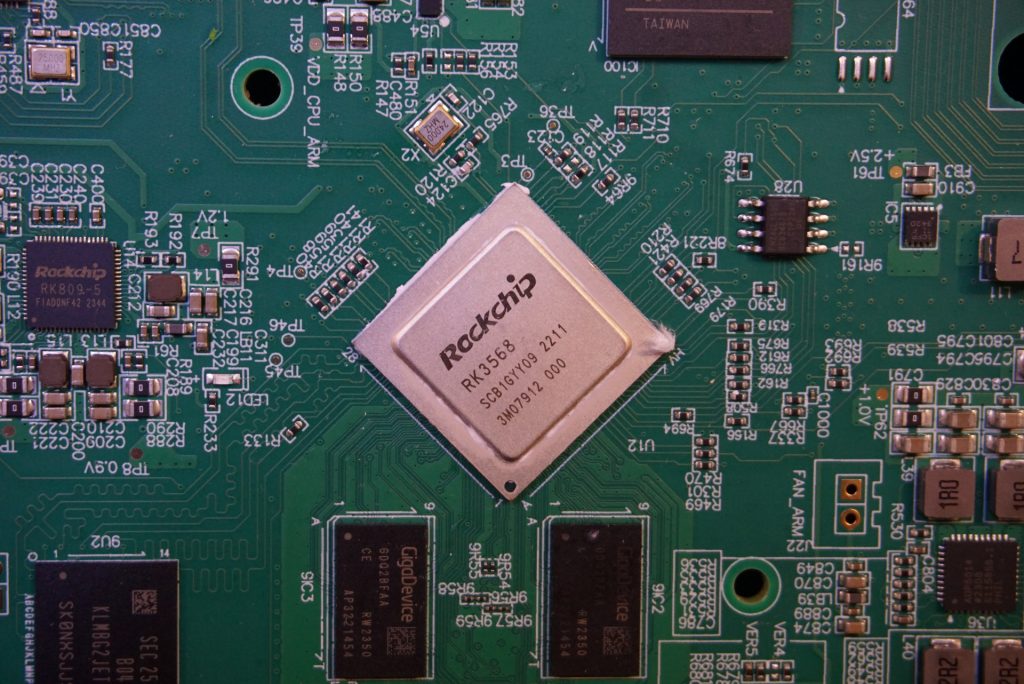
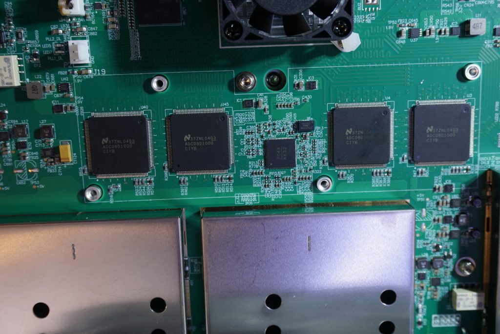
UNI-T used ADC08D1000 as the sampling ADC. The ADC08D1000 is an 8 bit dual channel 1 GSa/S ADC. It has a maximum sampling rate up to 1.3 GSa/S. Clearly to achieve the maximum 5 GSa/s sampling rate, you will need to have four of these ADC channels interleaved together. Thus two ADC chips are used to support a pair of input channels. Channel one and two share two of these ADC08D1000’s and channel three and four share the other two. When both channel one and channel two are enabled, the sampling rate would drop to 2.5 GSa/s as a result. So to achieve the full 5 GSa/s sampling rate in dual channel mode, you will need to select one channel from channel one or channel two and the other channel from channel three or channel four.
Between the ADCs there is an HMC7044 jitter attenuator.
In the picture below, you can see the Spartan-6 XC6SLX16 FPGA which is used to synthesize the signal outputs for the function generator. XC6SLX16 has 14,579 logic cells. The output DAC for the signal generator is an ADC9122, which is a dual 16 bit DAC.
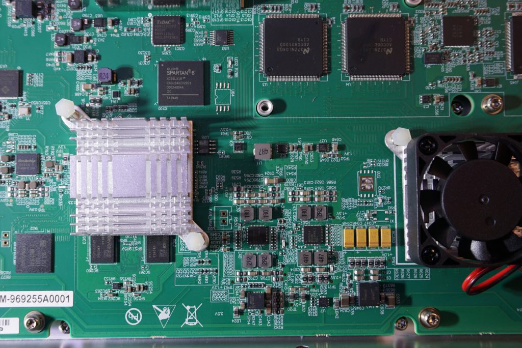
Between the application processor and the main FPGA, you can see two ADP5014 low noise buck regulator chips.
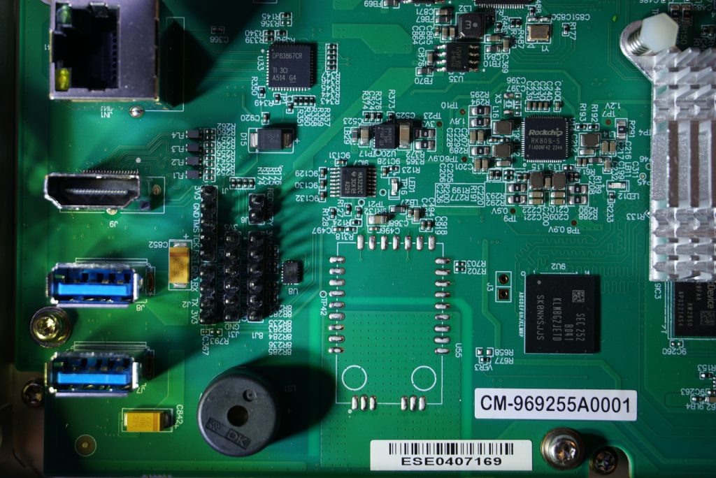
Here are a couple of pictures showing the bottom left side of the board. The missing component is for the WiFi module.
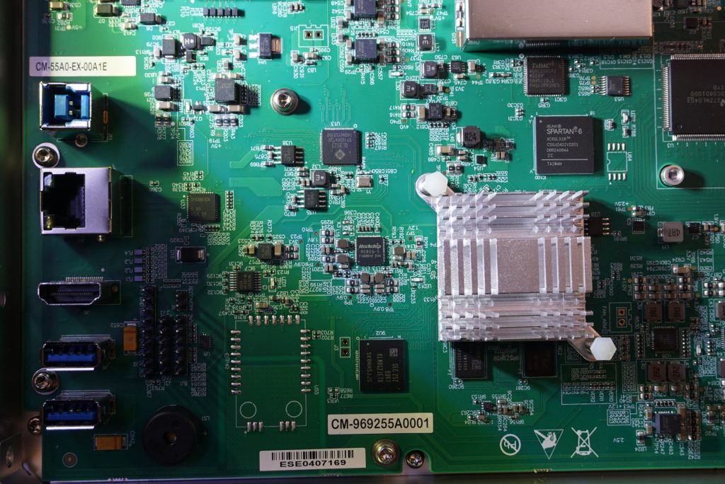
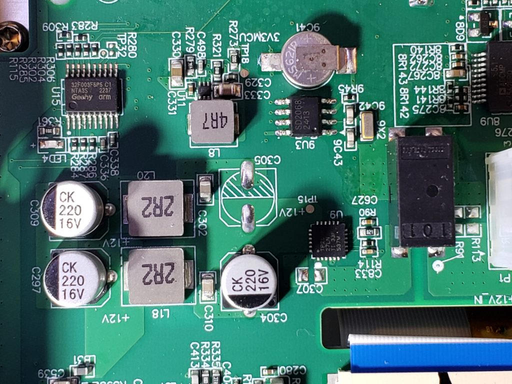
Towards the upper left you can see an APM32F003F6 MCU, an SD2068 RTC chip.
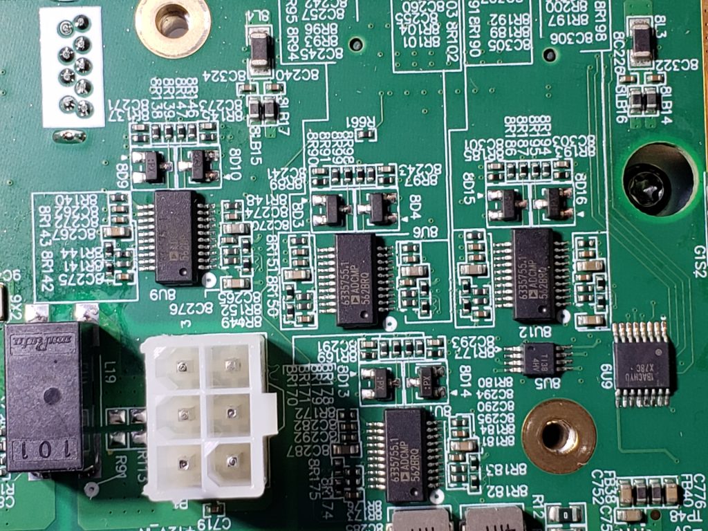
Towards the upper middle portion of the board, there are four ADCMP562 PECL high speed comparators which are used for the digital channels. There are four additional ADCMP562s on the reverse side of the board.
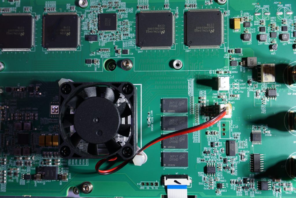
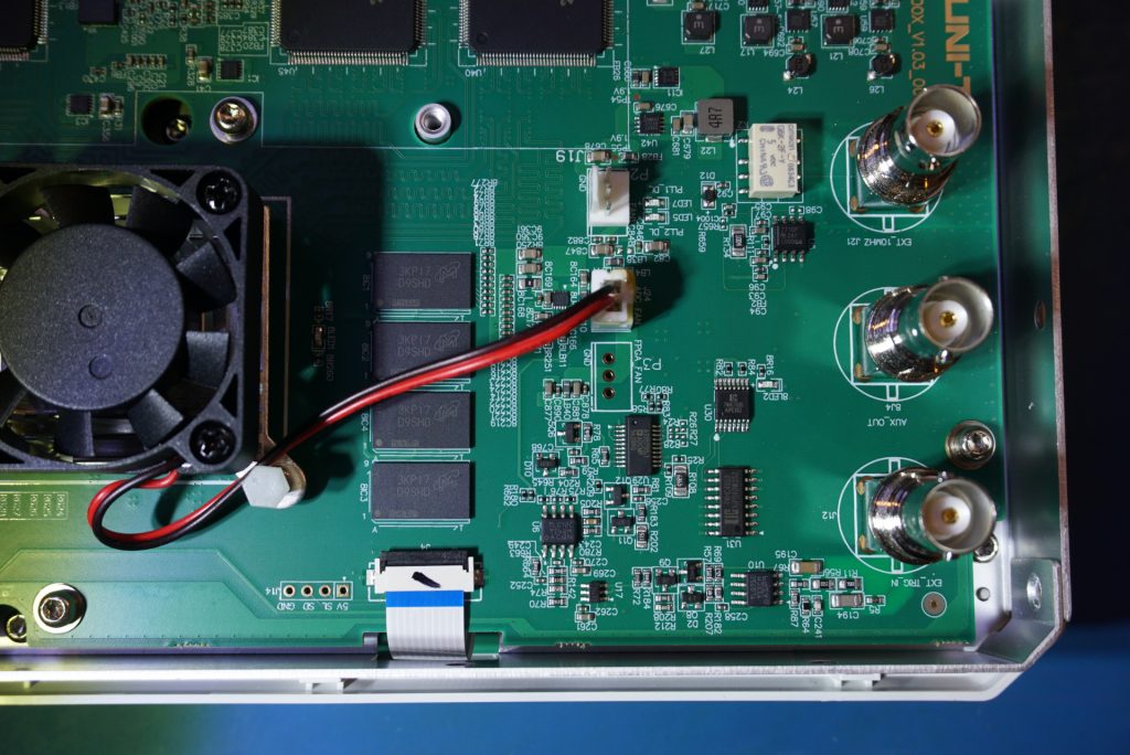
The the pictures below, you can see the sample memories and some miscellaneous circuitry around the BNC ports on the back of the unit.
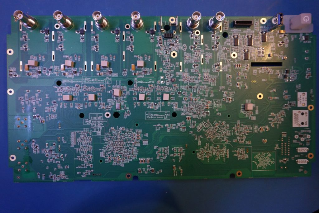
Here is a picture of the reverse side of the main board. Towards the middle, there is a TCXO for generating the stable clock signal
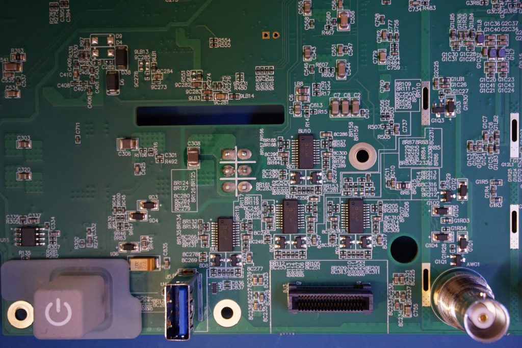
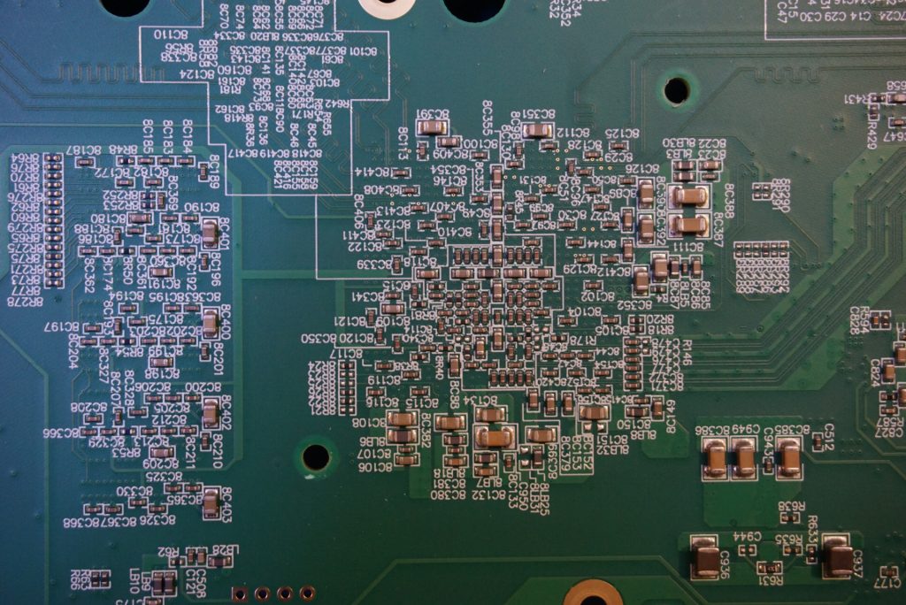
In the rst picture below, you can see the four additional ADCMP562‘s PECL comparators. In the other two pictures, you can see the decoupling capacitors underneath the main FPGA and the application processor.
Here is a picture of the assembled keypad input and BNC input boards.
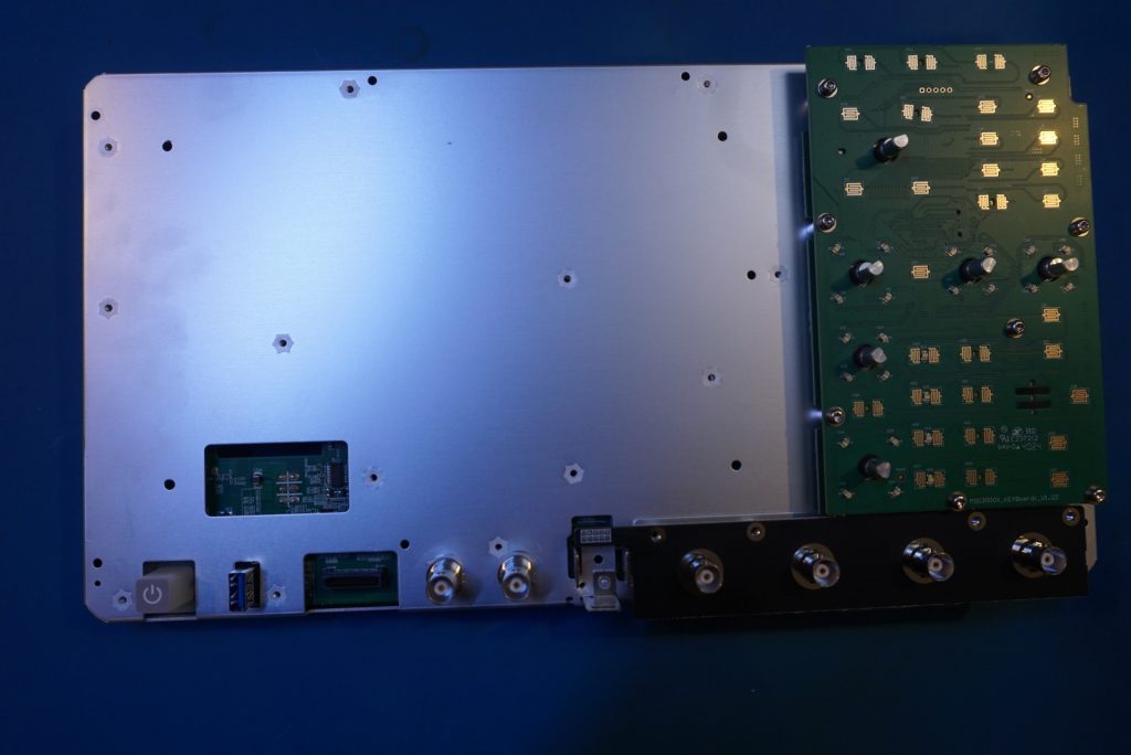
The key pad board is mated with the encoder board via header connectors.
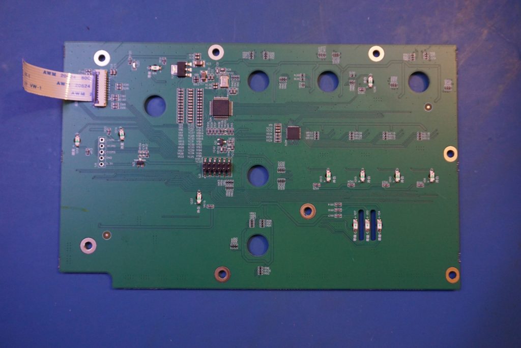
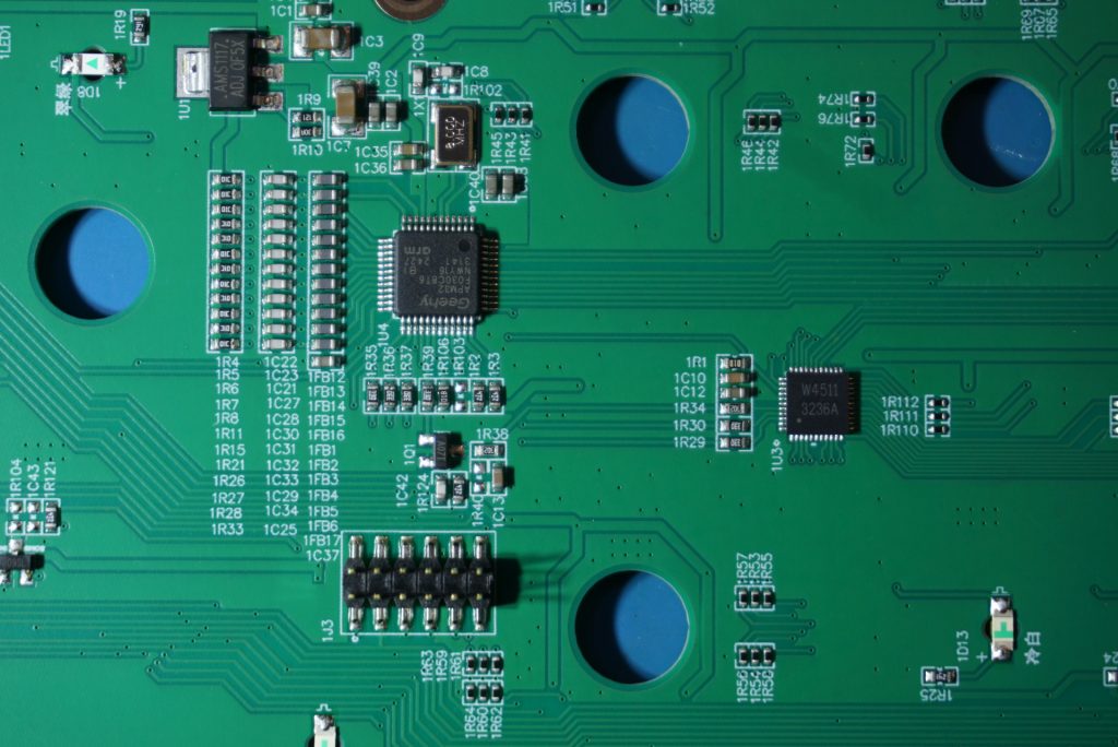
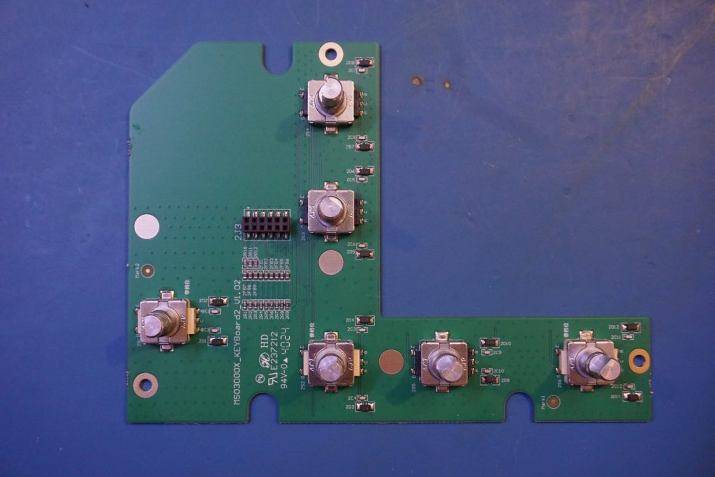
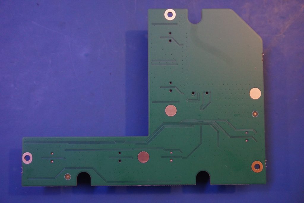
And here are a couple of pictures of the encoder boards.
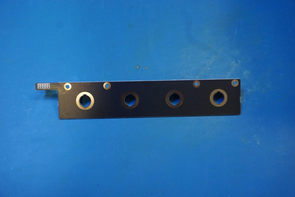
Here is a picture of the probe interface board. Since the MSO2000X series does not support active probes, this board essentially is just a ground plane.
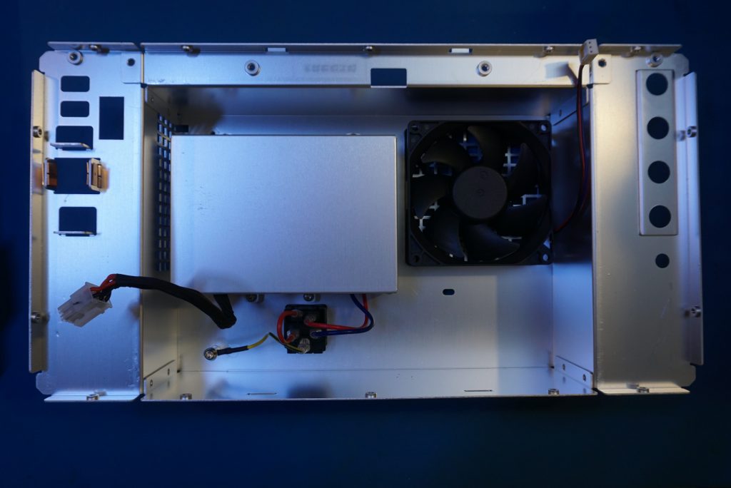
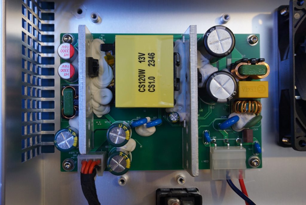
Finally, here are a couple of pictures of the back cover of the case and the main switching power supply.
And here is a link to the full teardown video:

