In my last blog post, I did a teardown of UNI-T’s UT8805E, a 5 1/2 digits benchtop multimeter. In this blog post, let’s take a look at what’s inside UNI-T’s UT8806E. I also did a detailed review video of the UT8806E, you can check it out in the video below if you are interested.
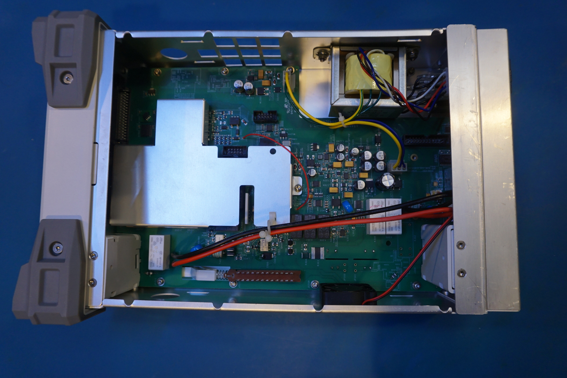
The overall layout of the UT8806E is very similar to that of the UT8805E. The layout is clean and there is a single PCB mounted at the bottom of the case. Like the UT8805E, the transformer is mounted on the side of the case for added rigidity.
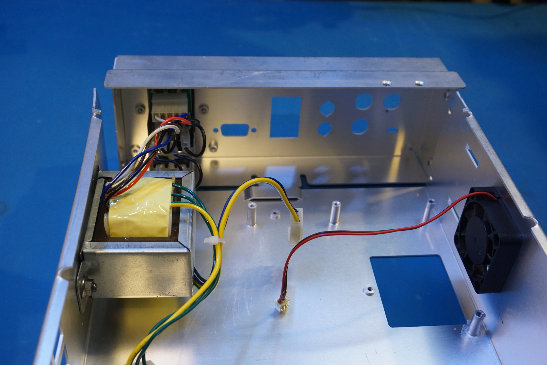
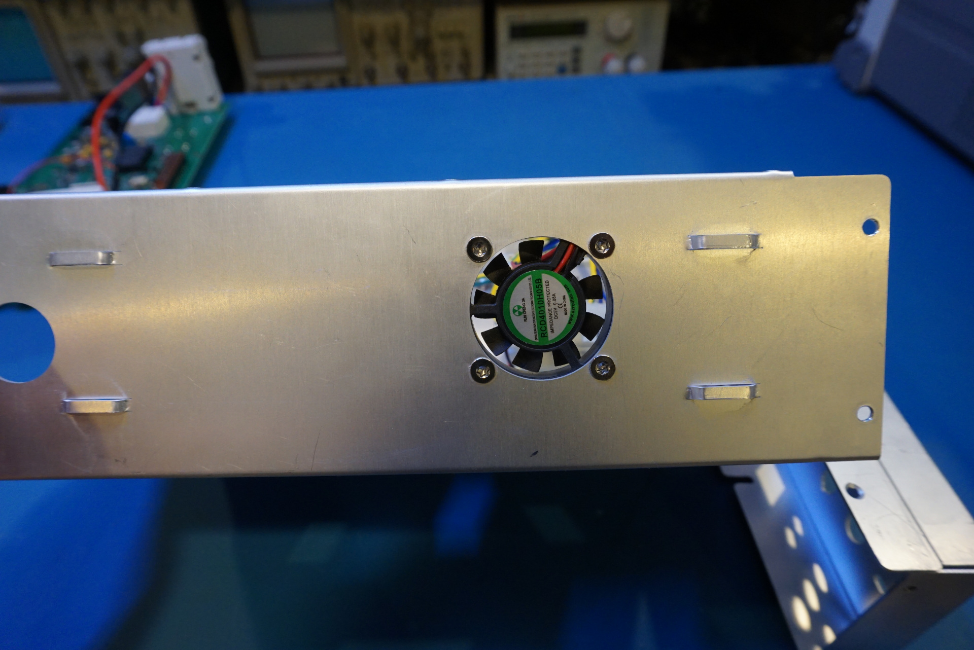
Here is a picture of the rear panel. Just like in the UT8805E, there is a cooling fan mounted on the side panel for forced air cooling.
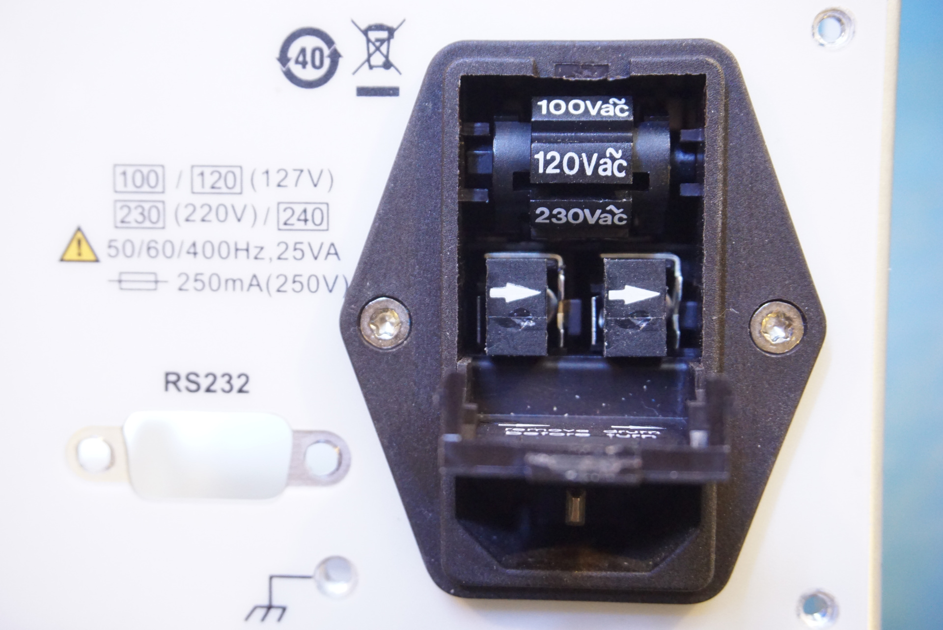
There are multiple windings on the primary side of the transformer and can accommodate mains voltages from 110V to 240V. The voltage selector is embedded in the IEC power entry assembly which can be seen in the picture to the left below:
Notice that the frequency of the mains voltage can be up to 400 Hz as this is designed to be able to work with aviation applications. To the right, you can see the fan used in the UT8806E. In UT8805E UNI-T used the same fan and it is fairly quiet.
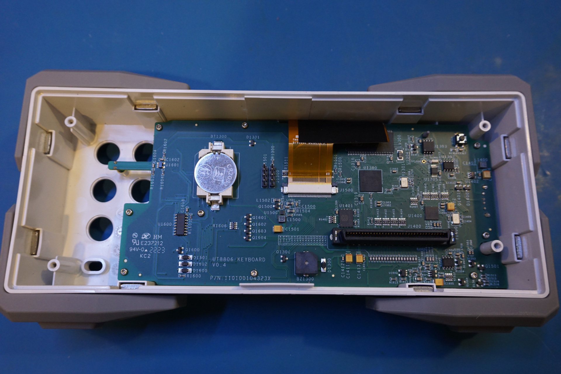
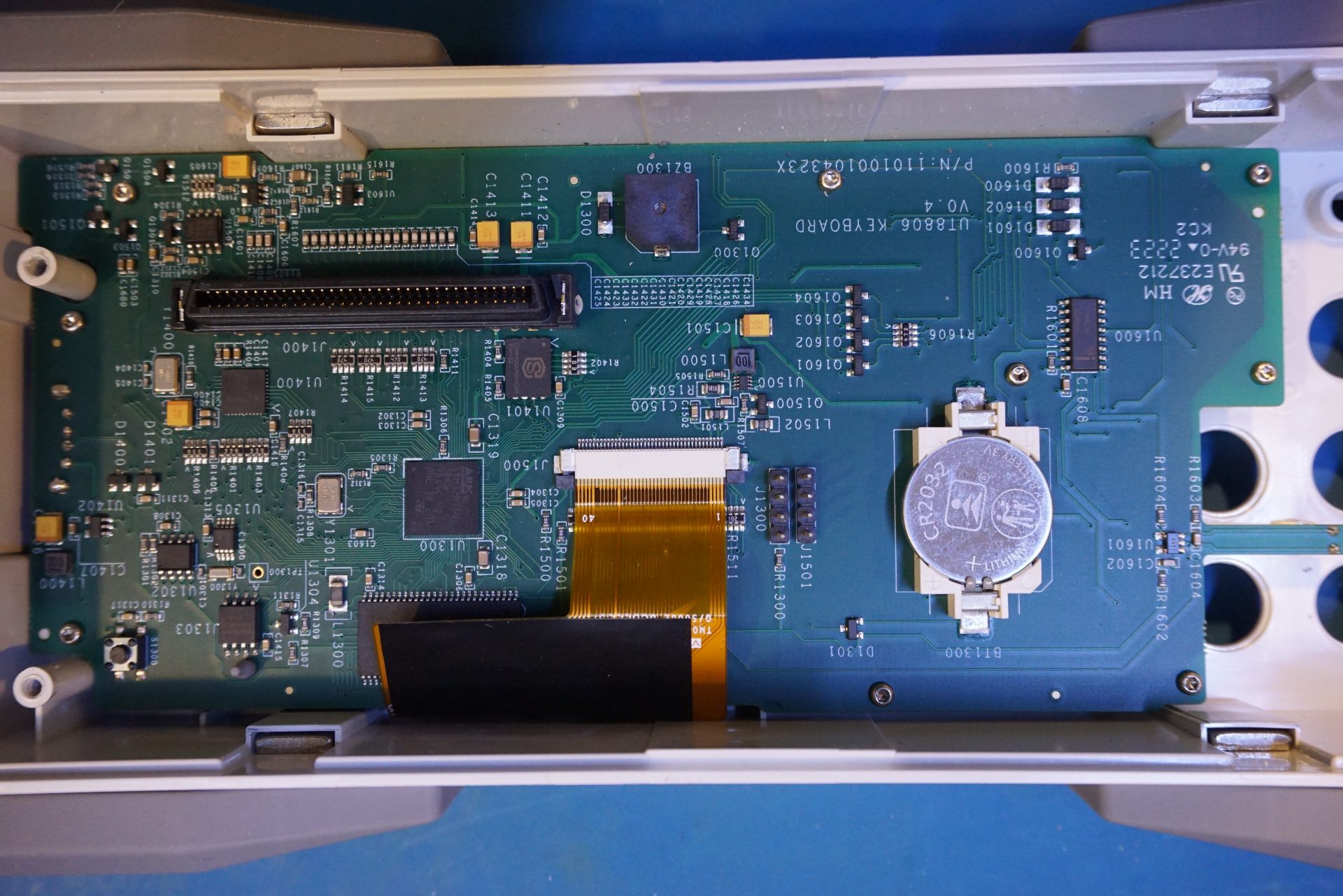
Here are a couple of pictures of the front panel PCB. The front panel is mated to the mainboard via a board-to-board connector. I had removed the metal bracket on the front panel assembly when taking these pictures. Unsurprisingly, the MCU used is an ARM STM32F750, which is has an ARM Cortex-M7 core.
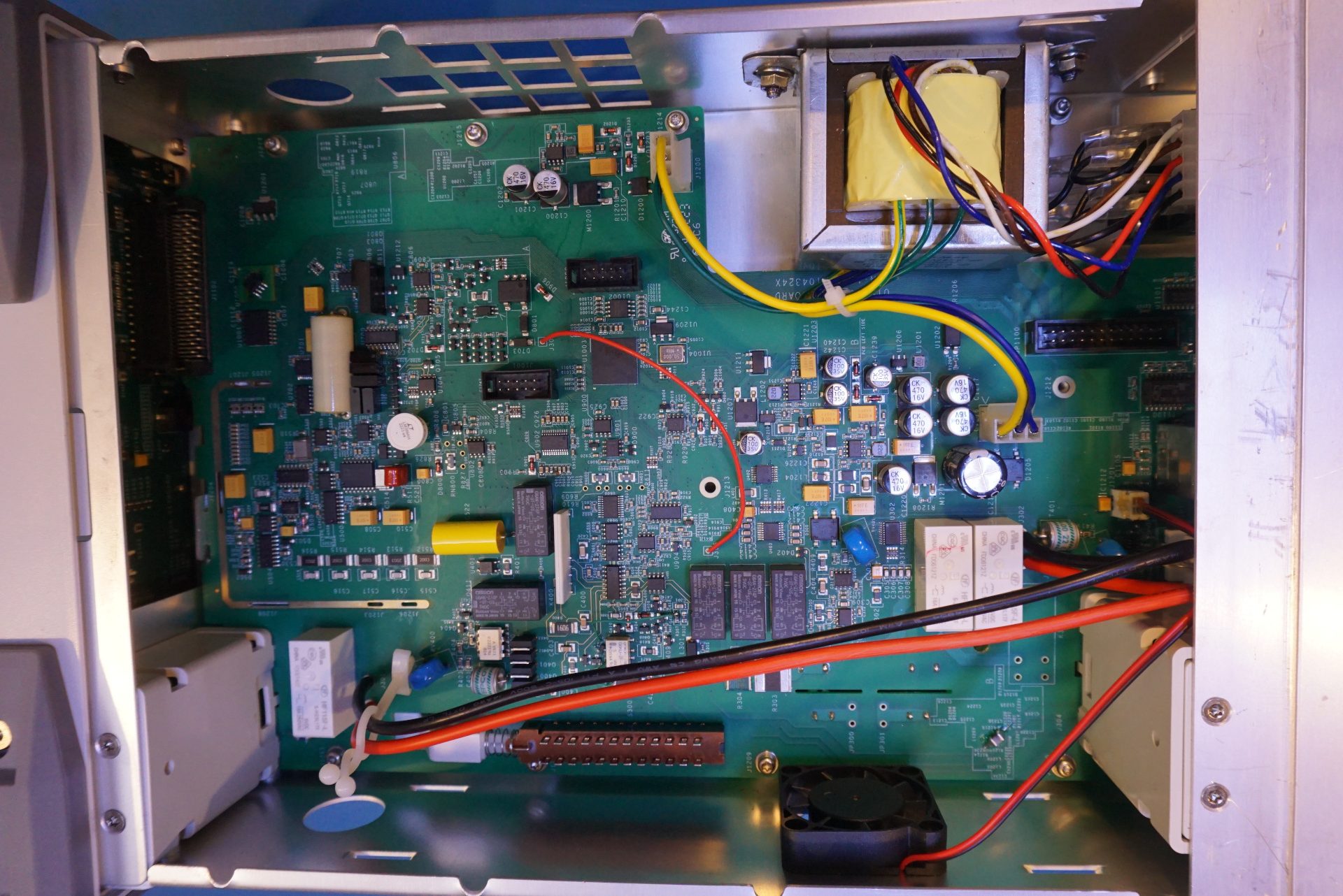
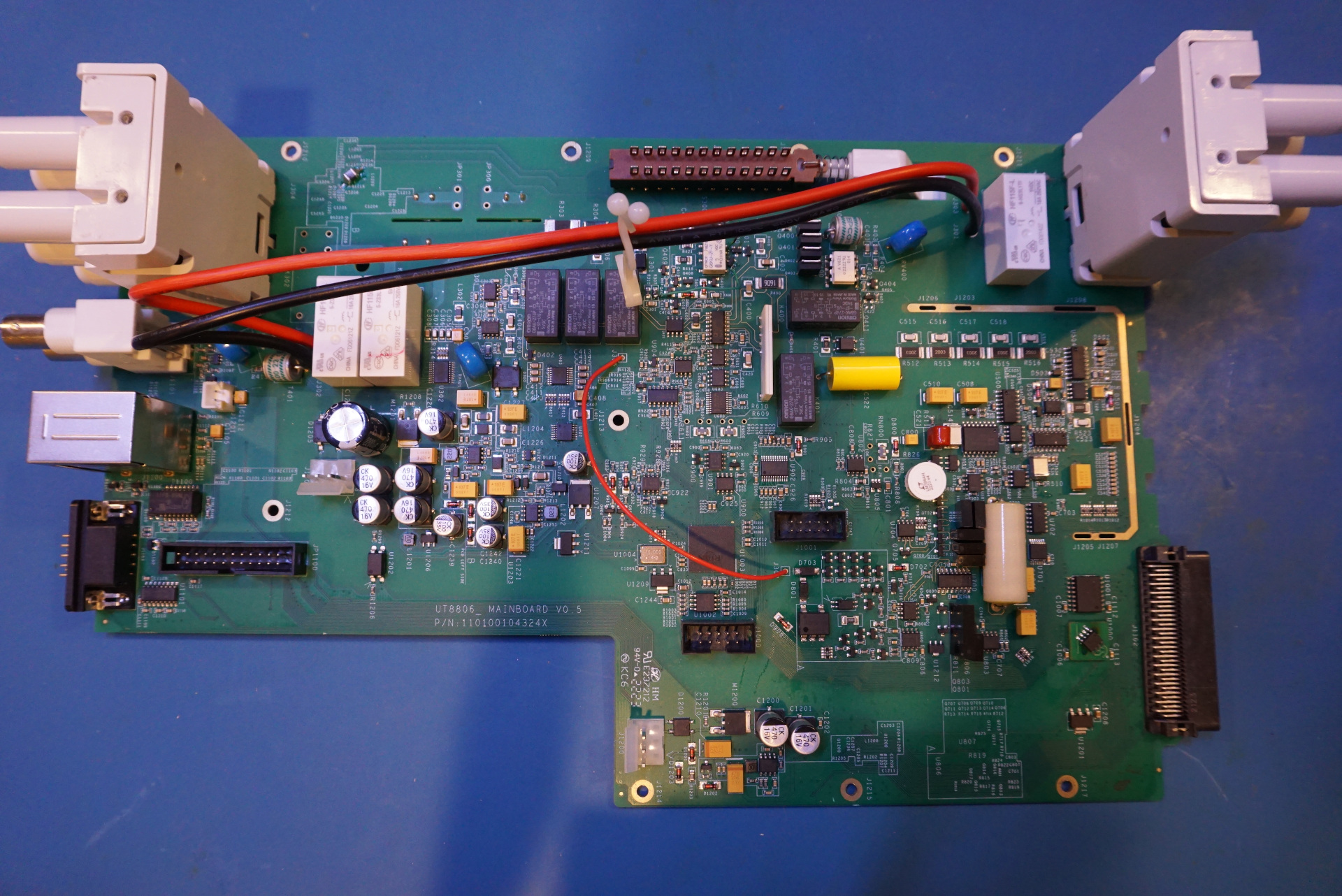
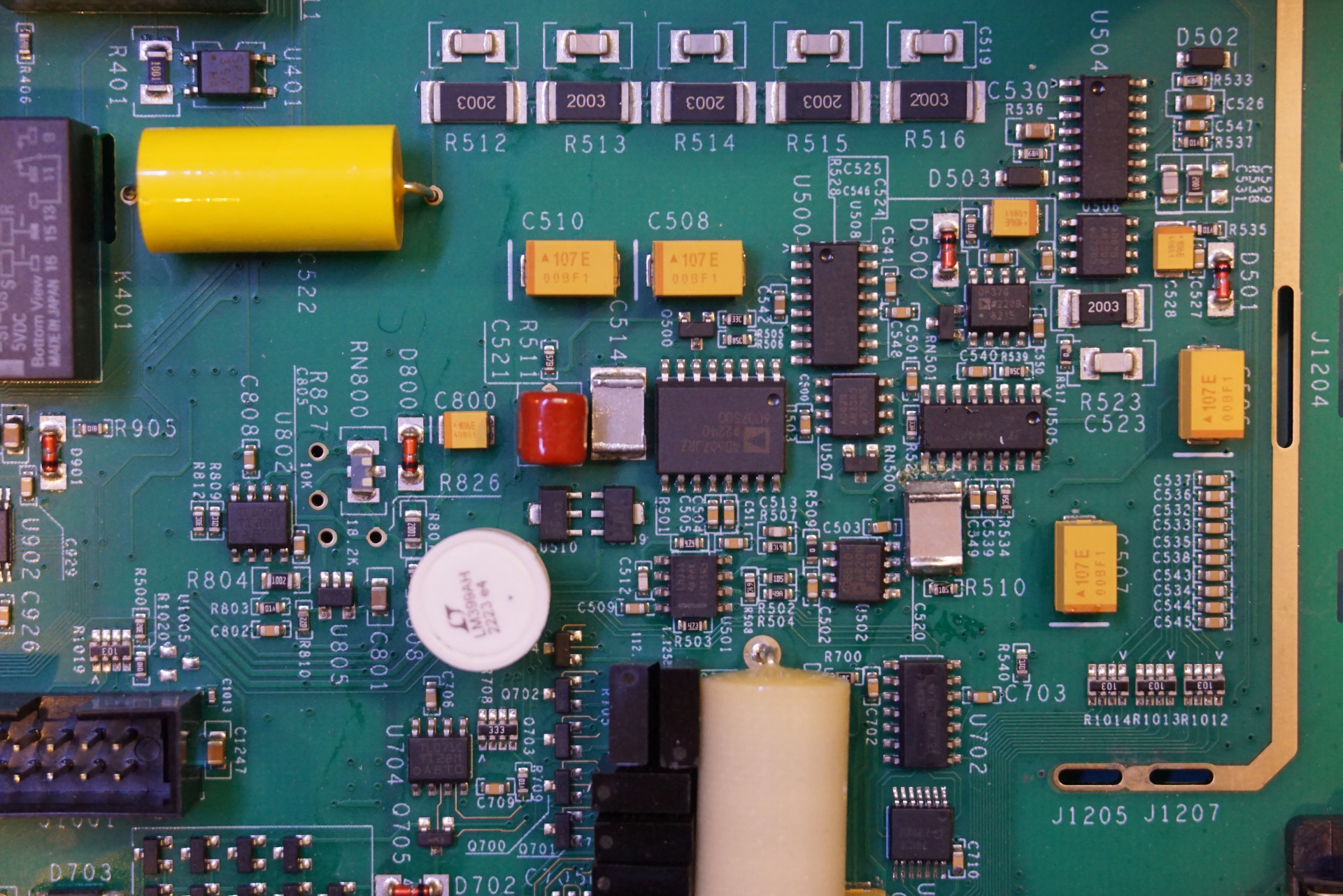
And here are a couple of pictures of the main PCB after it has been removed from the case. In the picture to the left below, you can see two sets of input jacks, one for the front panel input and one for the rear panel input. The thick wires connecting the front panel and rear panel are for the high current range current measurement. They are switched by the relays. And the rest of the jacks are switched by the ganged switch from the front panel.
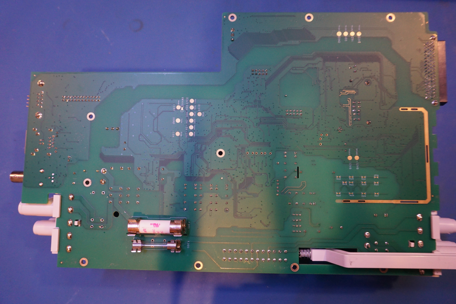
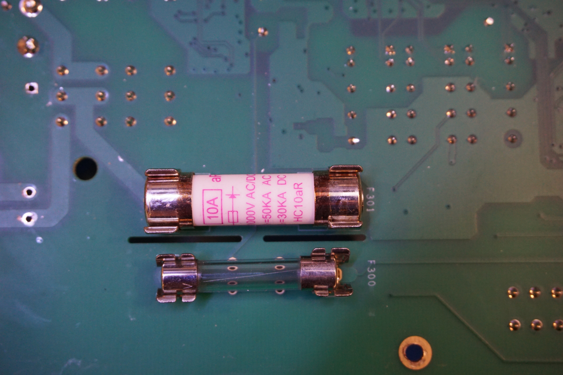
Here is a close up picture of the fuses used in the meter. They are for the lower current range and high current range. The fuses are located at the bottom side of the PCB and can be accessed by removing a panel door at the bottom of the case. There is a plastic cover over the fuses which creates a physical barrier between the high current fuse and the low current fuse. In the event of a fuse rupturing, it will be contained within the individual fuse compartment.
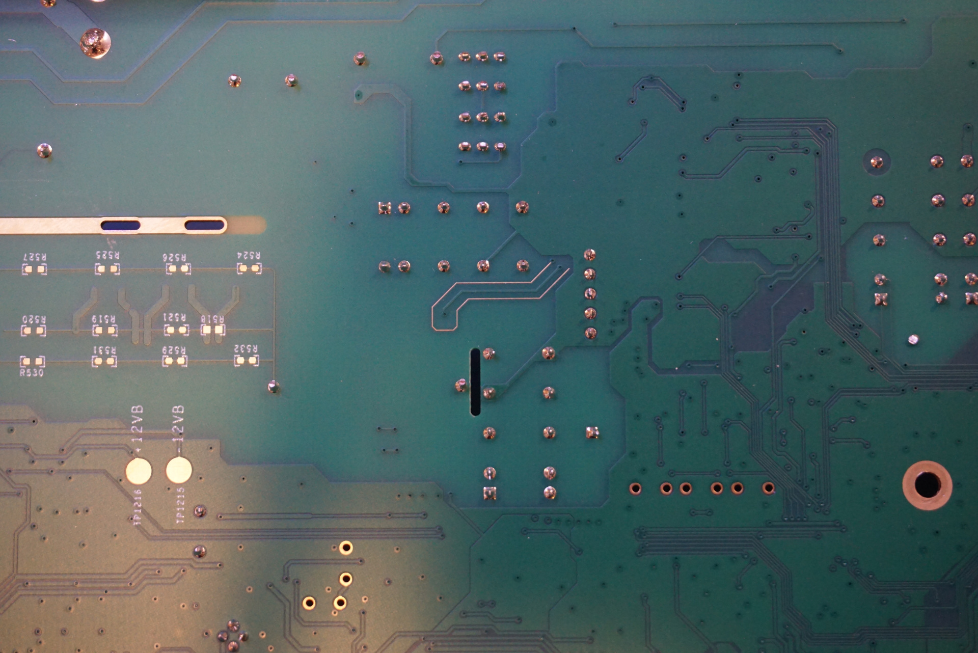
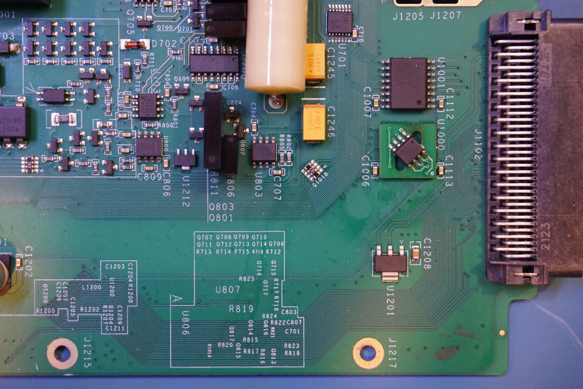
In the picture to the right above, you can see a guard trace surrounding a signal trace. And there are some unpopulated resistors on the reverse side. They may be reserved for the alternative footprints for the input resistor string which is populated on the top side.
Just like in the UT8805E, a Caddock 1776-C68 voltage divider resistor network is also used in the UT8806E.
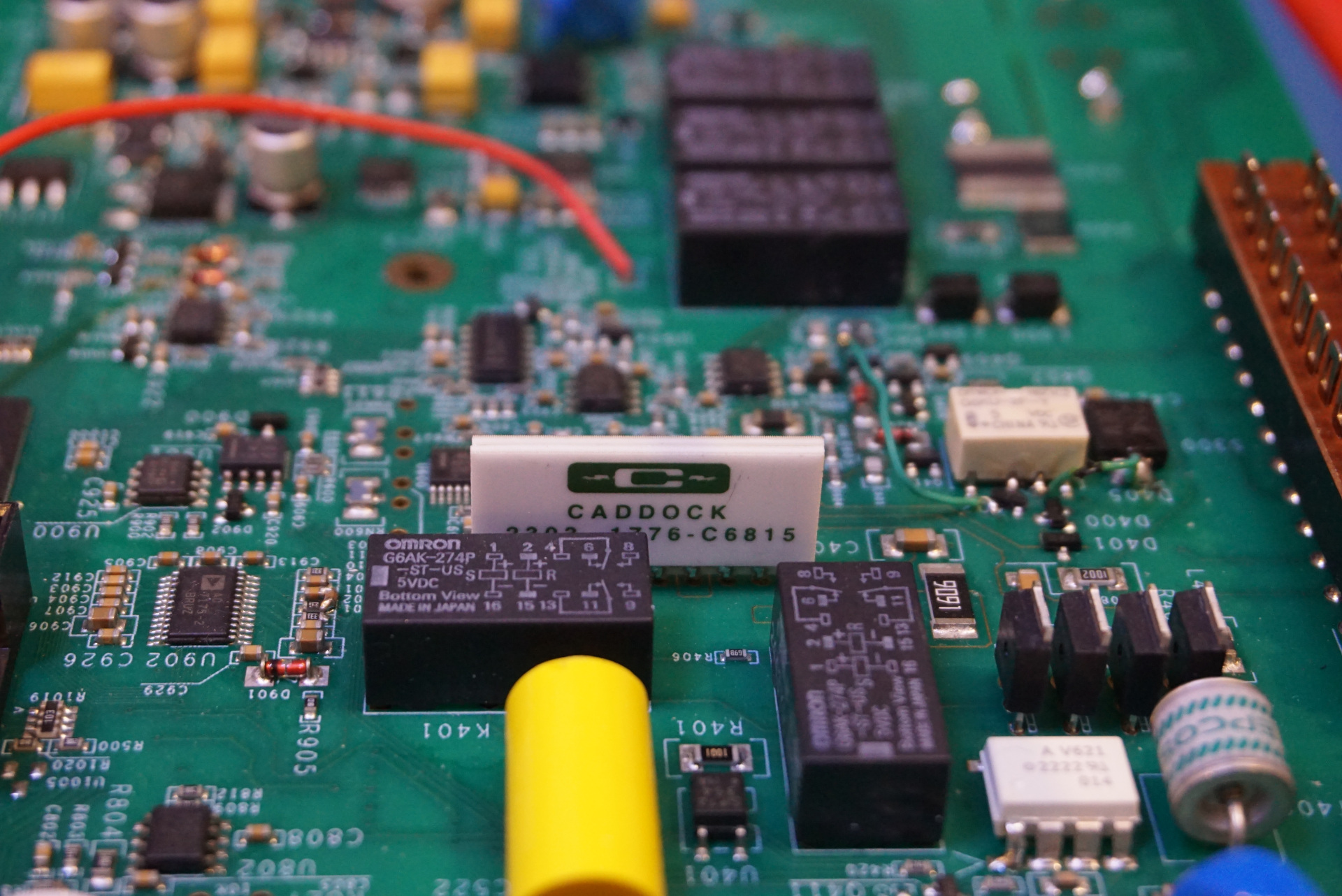
In the picture above, you can probably spot the bodge wires around the relay. Here is another picture showing the bodge. You can also see some guard traces in that section. To the upper left that’s the main current shunt used for the 10A range and a 1 Ohm precision resistor used for the low current range.
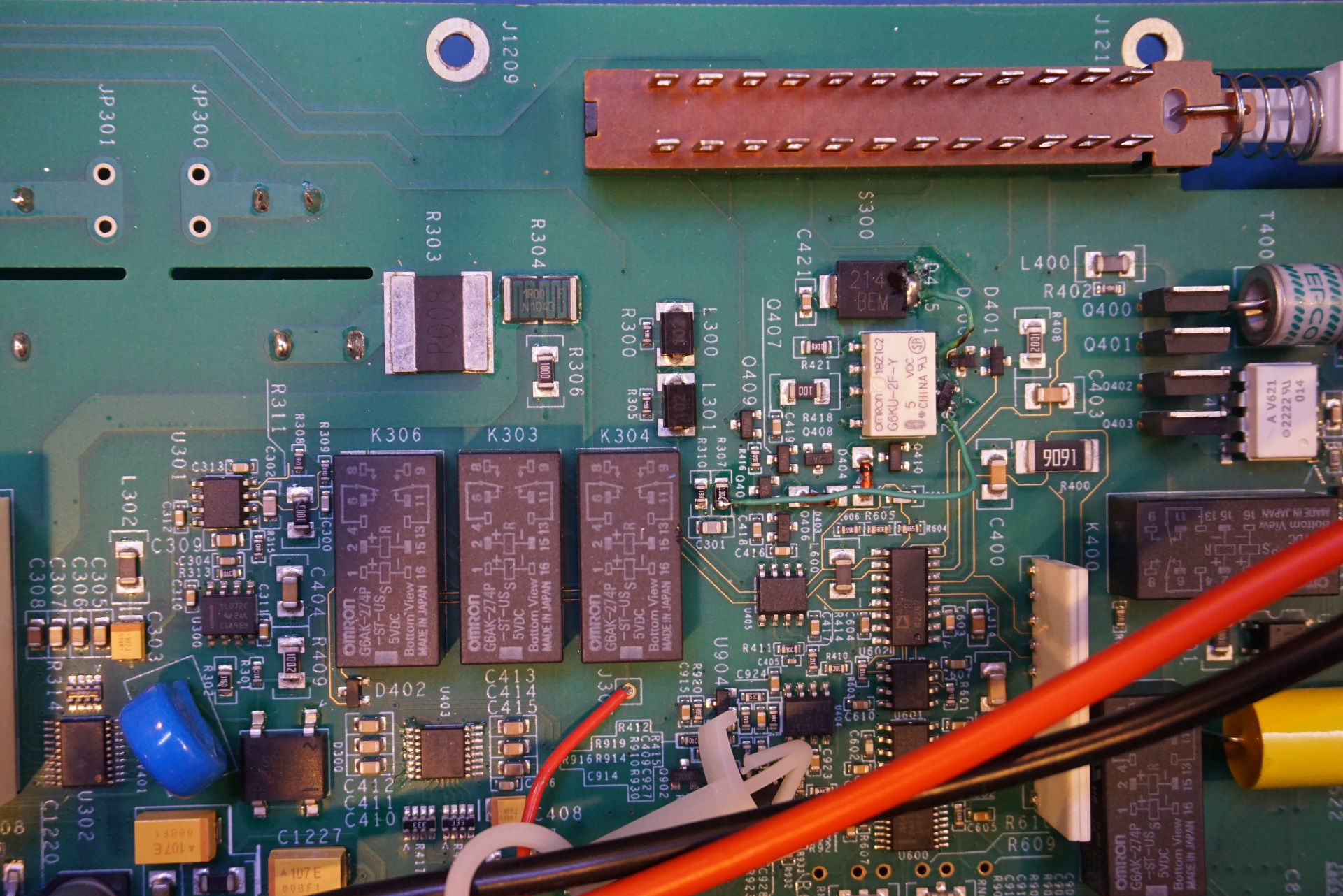
Keep in mind that the unit I have is from the early production runs, so the budge wire may have been fixed by UNI-T later on.
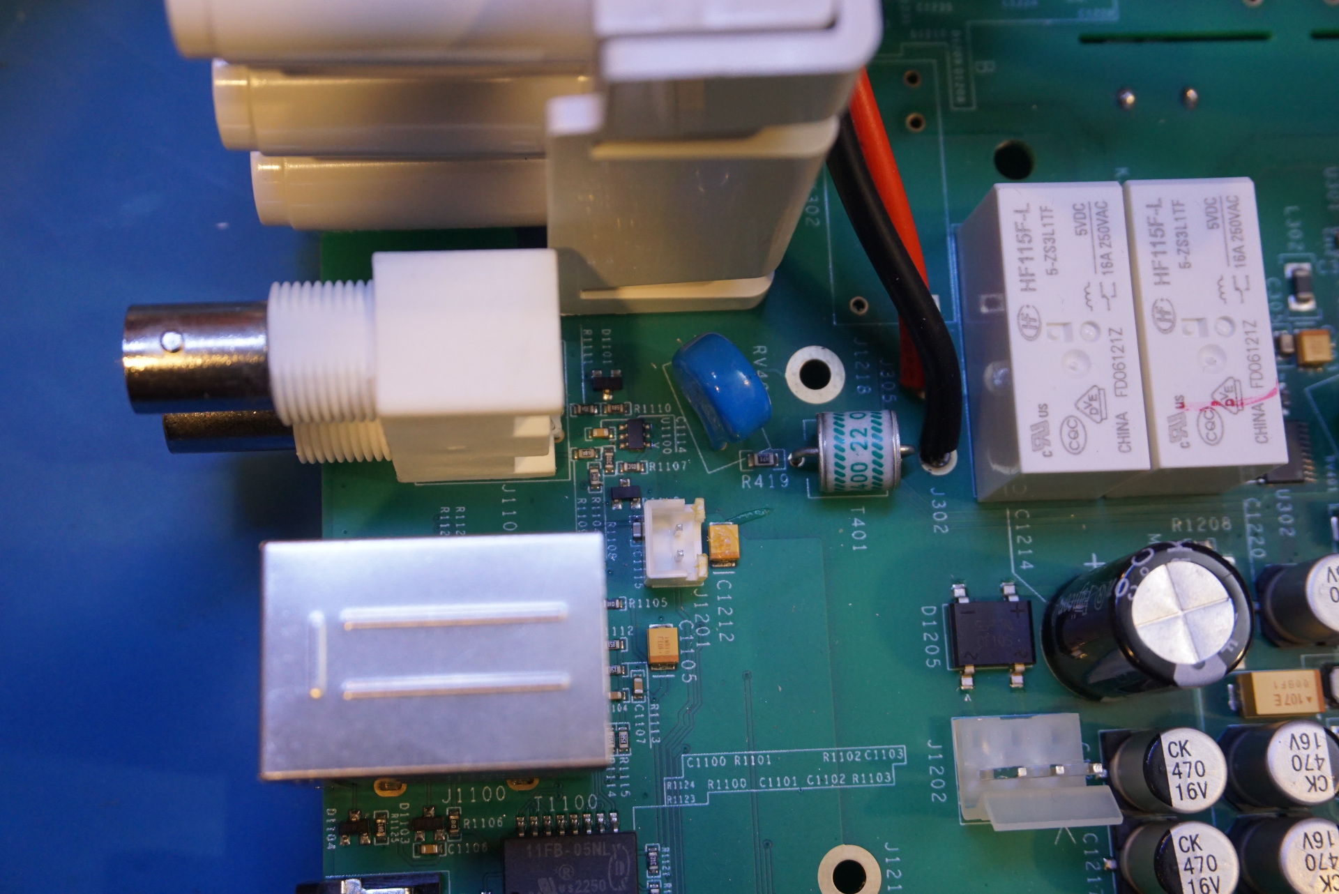
Discharge tube is used for transient clamping. There are a couple of gas discharge tubes used on the 8806E, one for the front panel input and the other for the rear panel input. You can also see the MOVs in the pictures below. The picture to the right contains the circuitry for voltage regulation and the fan blows across this area.
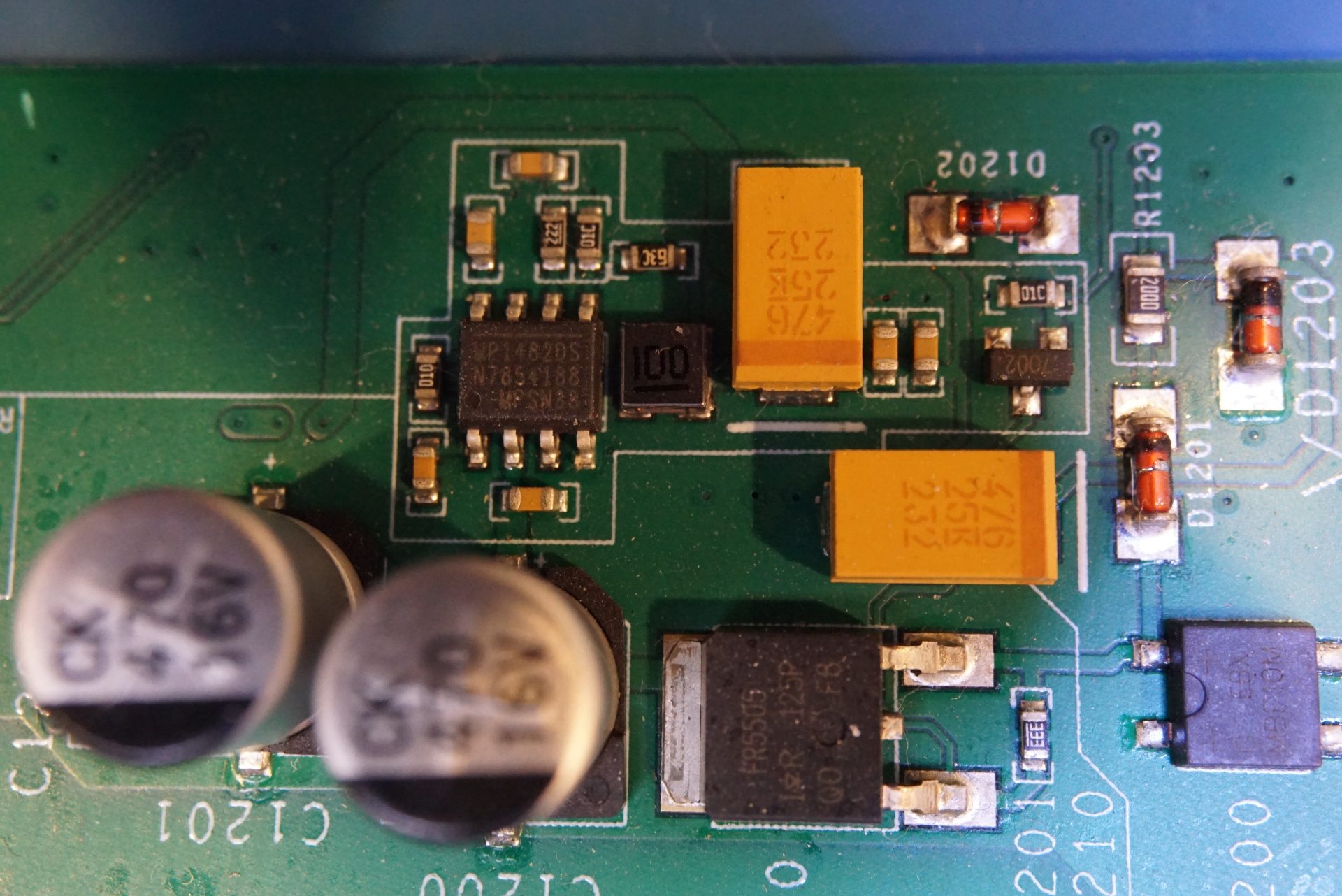
Unlike the voltage regulators used in the 8805E, none of the linear regulators used in this unit is on headsinks. And if you look closely, you can see some inductors. So I suspect UNI-T is using a mixer of switching regulators and linear regulators to lower the overall power dissipation. This is rather unusual to see inside a 6 1/2 digit multimeter.
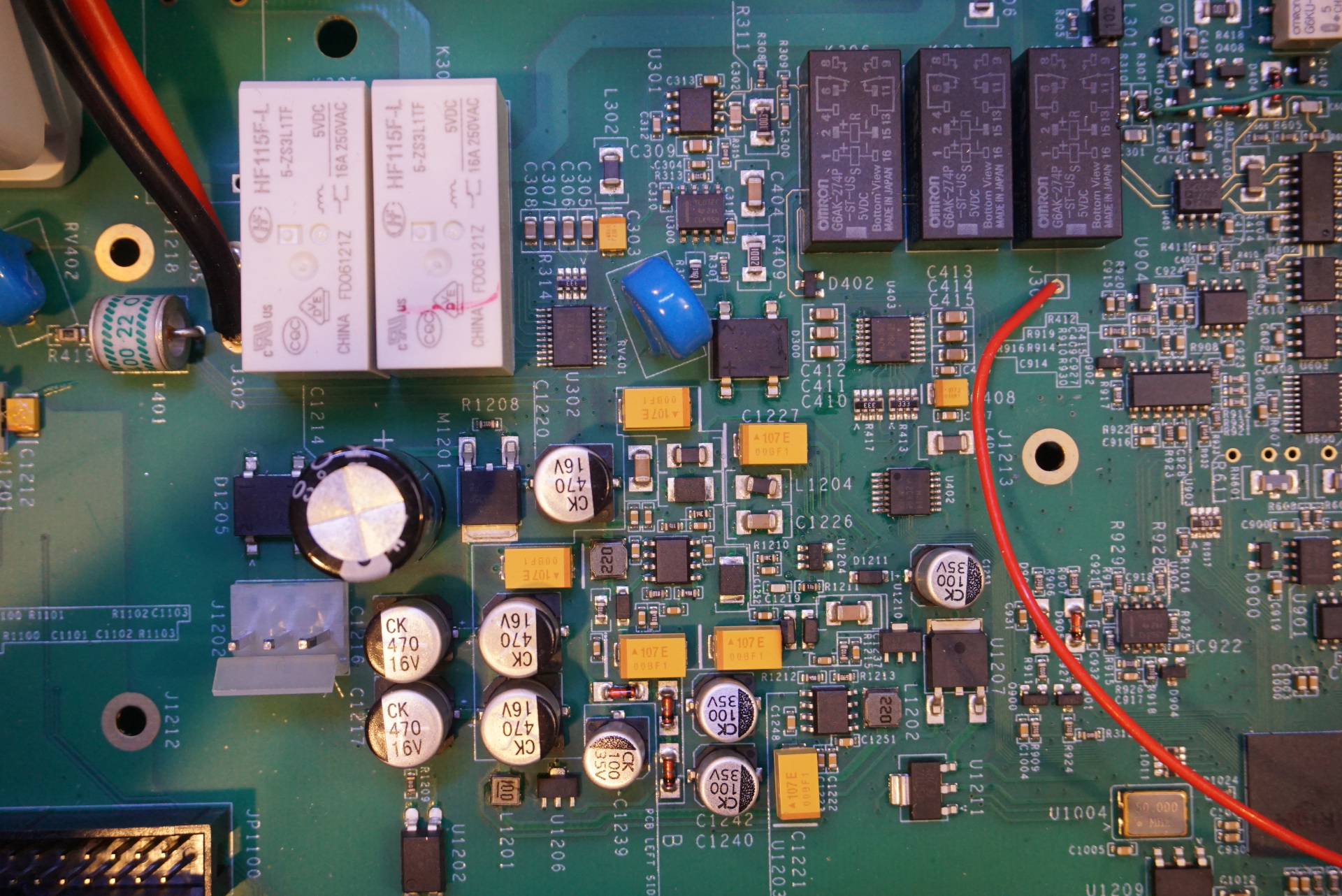
And here you can see another buck converter, MP1482DS, used for powering the front panel.
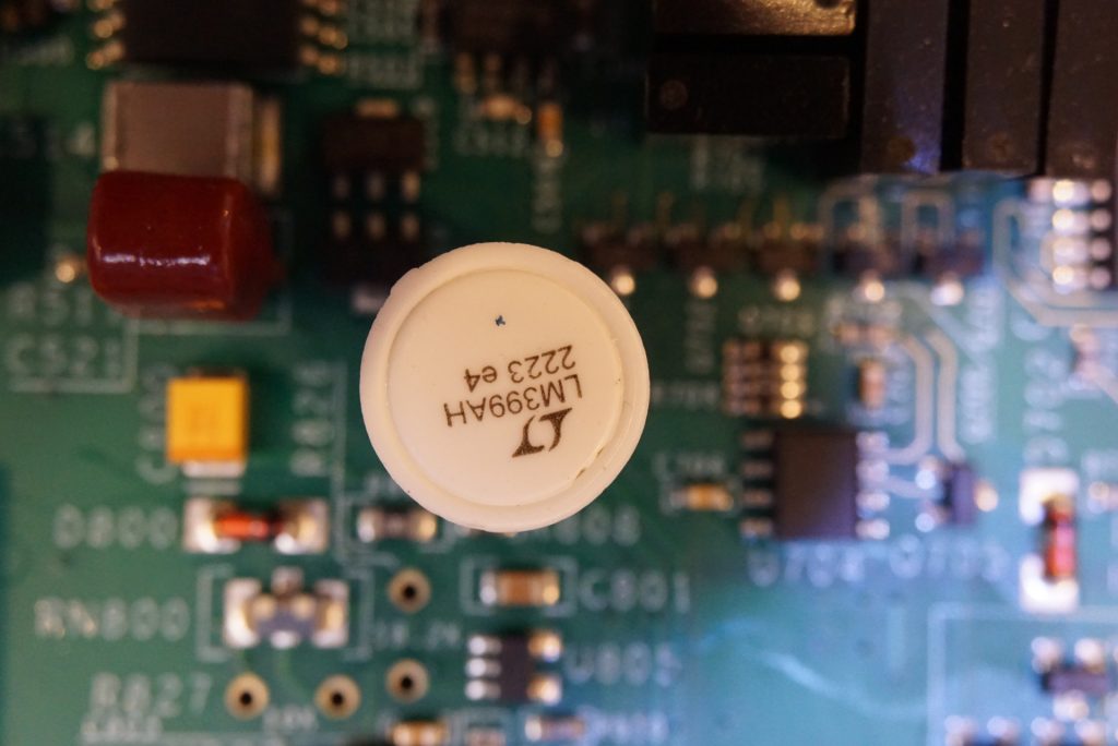
Here is a close-up of the voltage reference used in the UT8806E, it is an LM399:
And here is a close up of the RMS to DC converter used, it i san Analog Devices AD637:
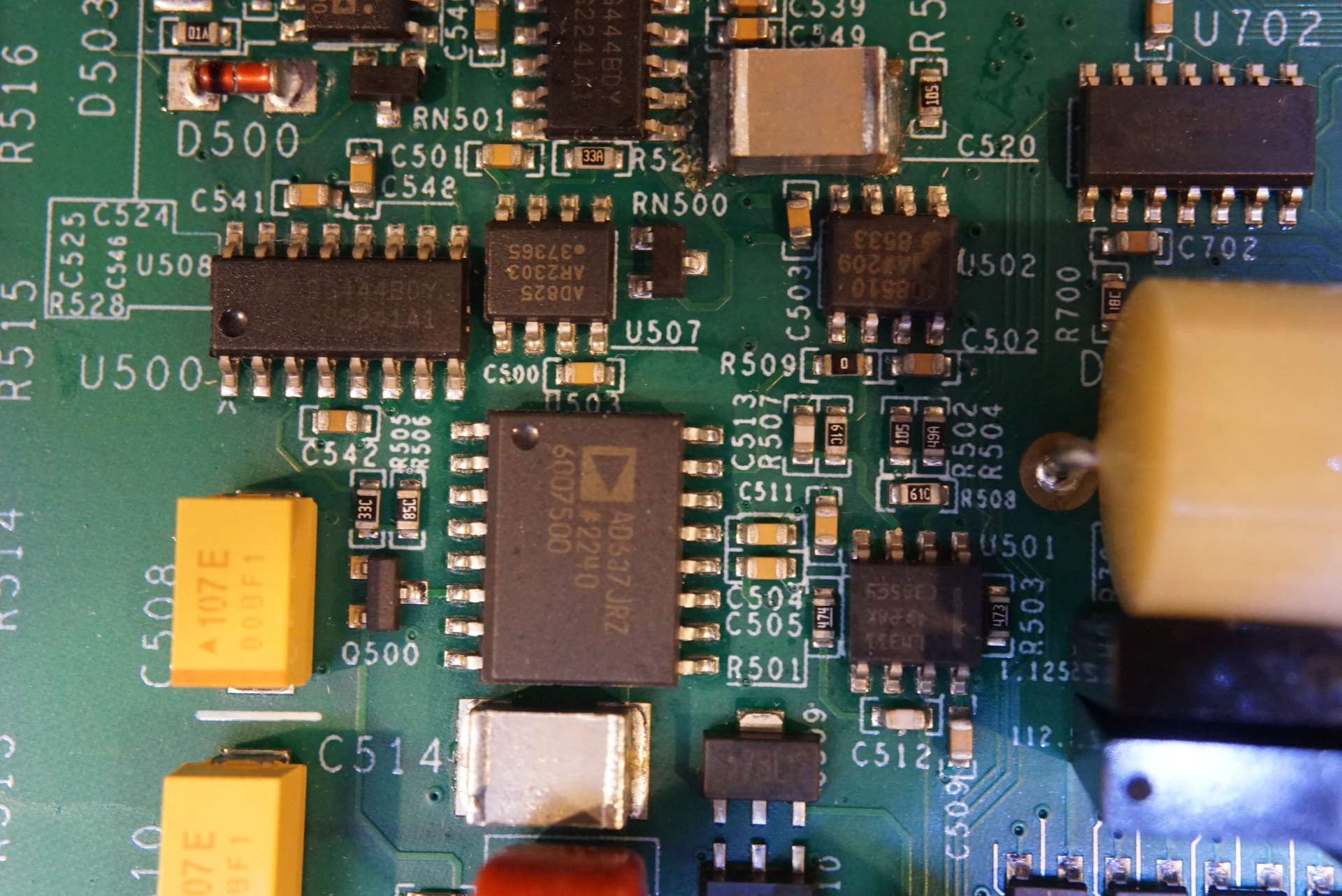
Here is a zoomed out picture giving you a general idea where the AD637 and LM399 are located on the main PCB. In the picture below, you can also see the resistors (200 k) in series forming the 1 mega Ohm resistance. Each of the resistor has a capacitor connected in parallel for tuning the frequency response. If you recall, I showed earlier on the other side of the PCB there were some unpopulated resistors. Presumably, those are reserved for different footprints.
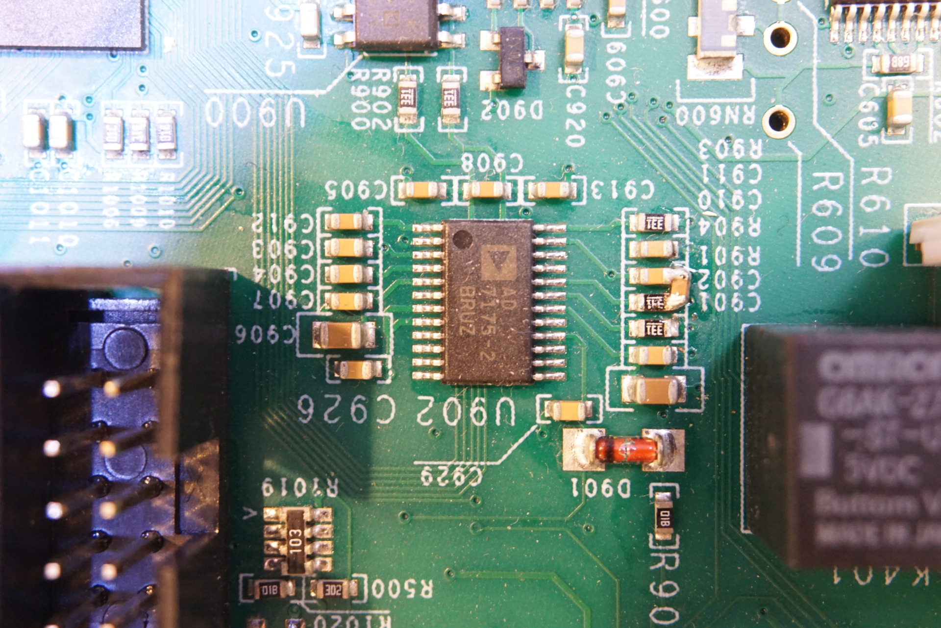
The main ADC used in the 8806E is an AD7175-2, which is a 24 bit 250 kSPS Sigma-Delta ADC. In the 8805E, UNI-T used an AD7172-2. The AD7172-2 has a 31.25 kSPS sampling rate which is already insanely fast. The ADC used in the 8806E is even faster. Can you spot the bodged capacitor below?
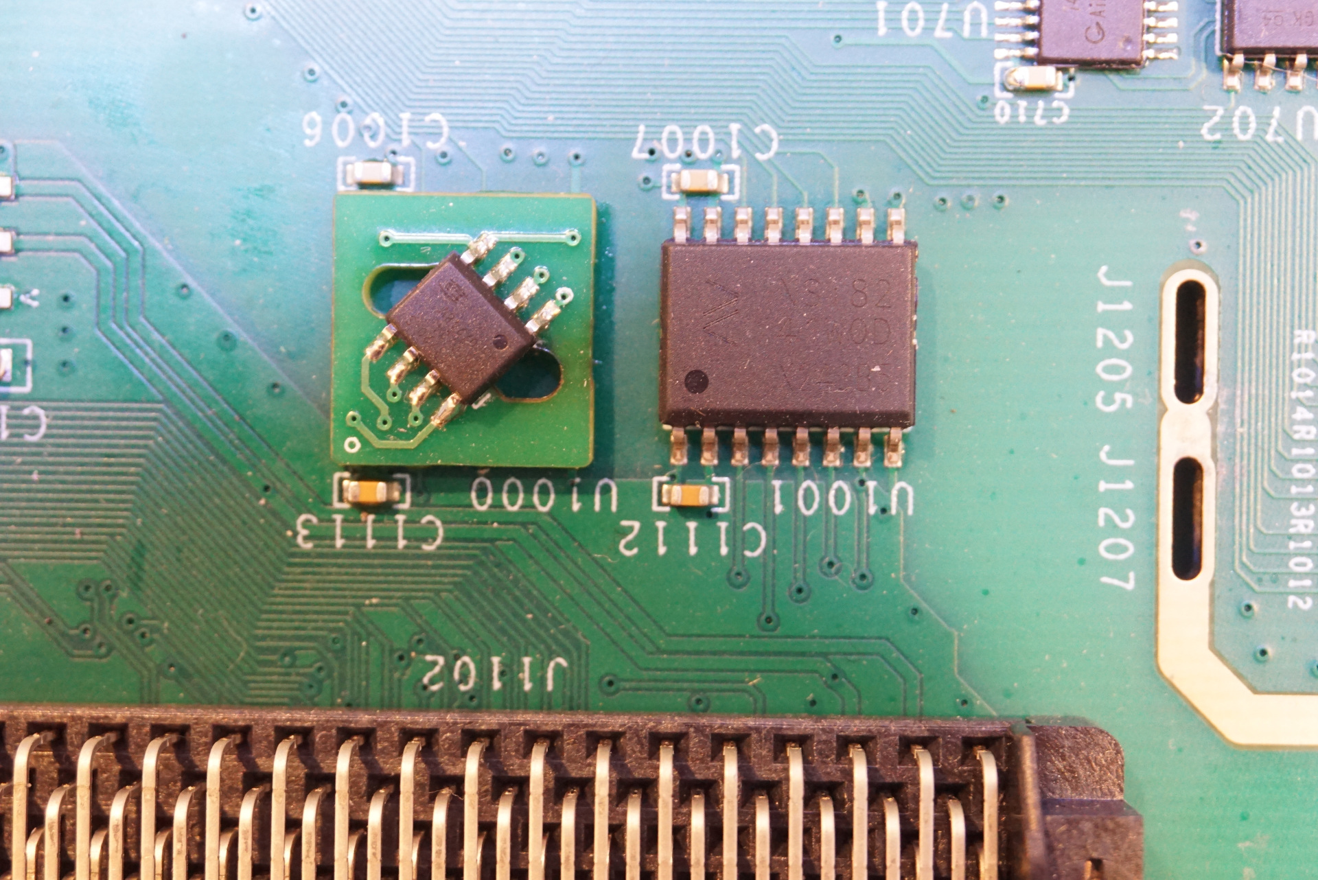
Unlike in the 8805E, there are two different input isolators used, and there is no isolation slot on the main PCB. I wonder why UNI-T chose to use two different isolators and one of which is mounted on a daughter board.
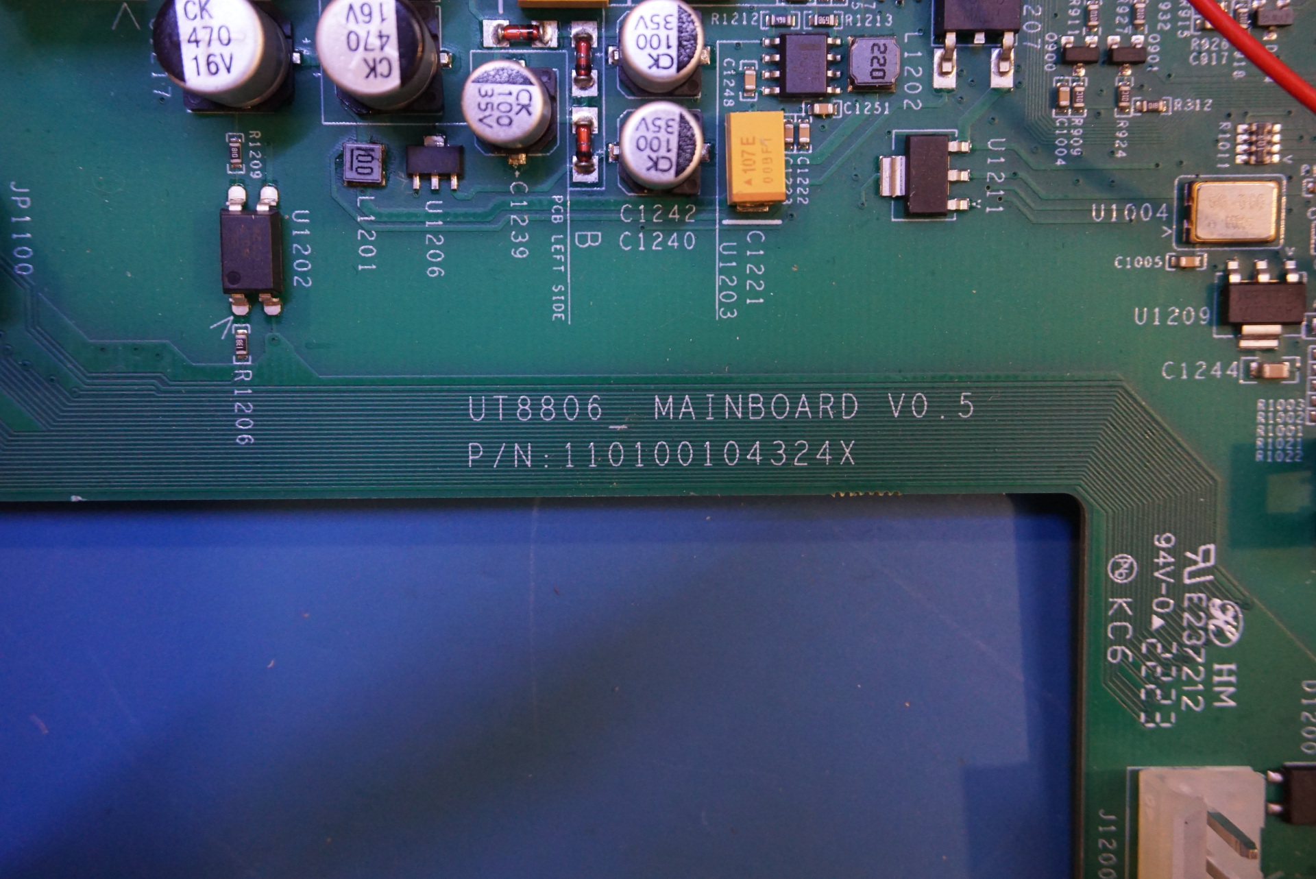
In case you are wondering, here is the main PCB version:
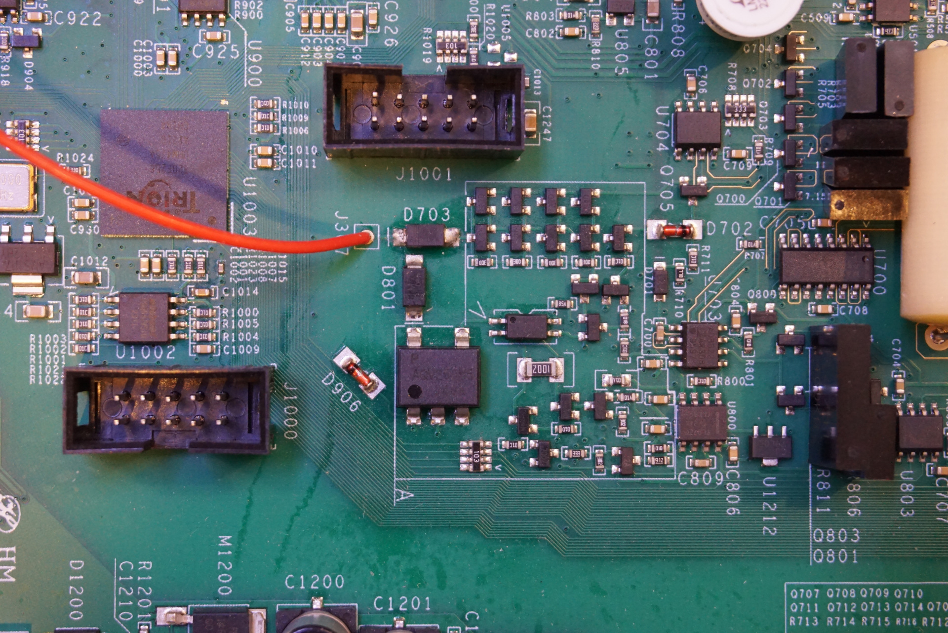
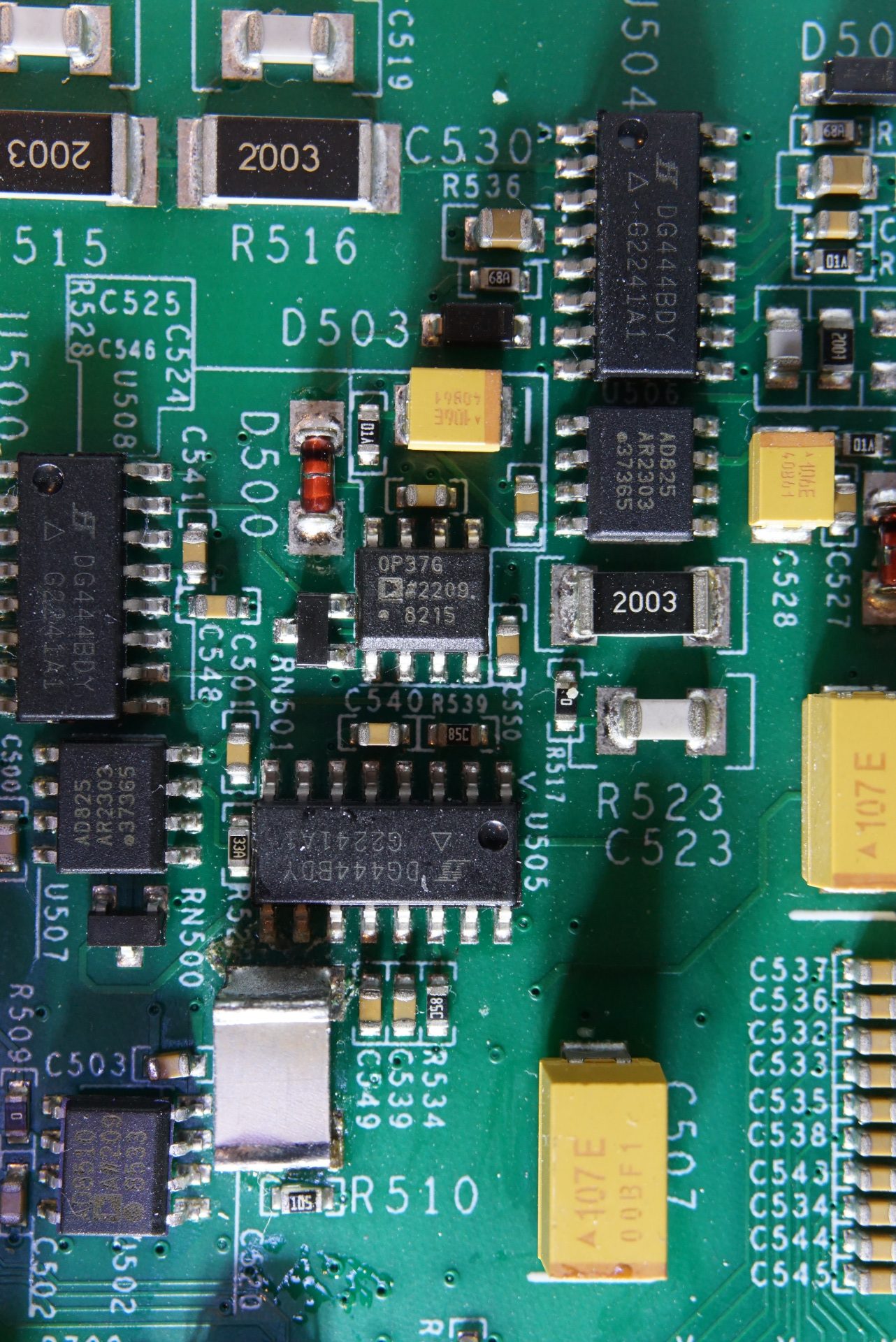
In the picture to the left below you can see the main FPGA from TRION. And in the other picture you can see some of the components used (AD825, DG444, OP37G) etc.
Here is a video of the teardown:

