I reviewed UNI-T’s 5 1/2 digit UT8805E bench meter a few weeks ago. In this blog post, let’s take a look at some of the teardown pictures.
The UT8805E utilizes a single board design, the layout is very clean. The power transformer is mounted on the ridged side panel which gives it the maximum structural strength.
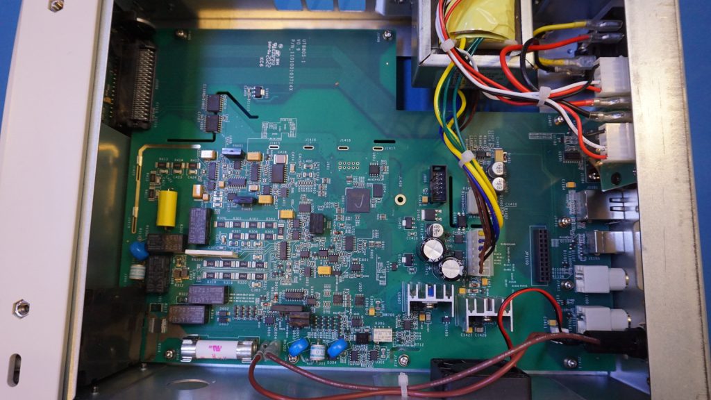
Here are a couple of pictures showing power entry module and the connectivity options on the back panel. The riser board is for adjusting the mains input voltage. You can see the GPIB cutout which is unpopulated on this model. The fuse on the right is for the low current measurement range.
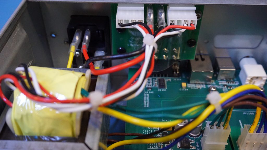
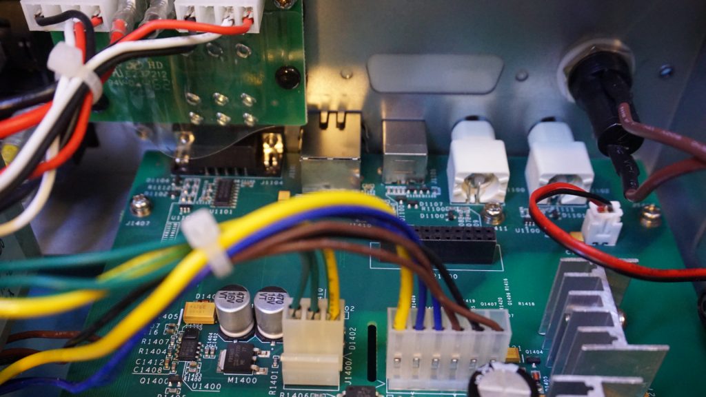
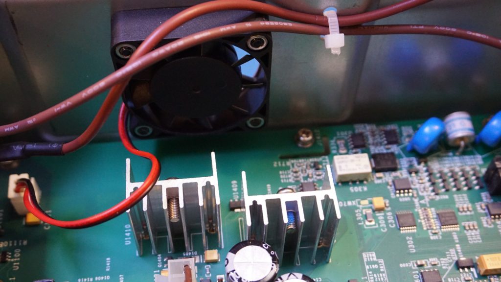
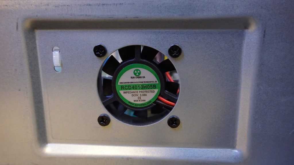
The UT8805E has a cooling fan. It is used for the cooling of the onboard linear regulators which can be seen in the picture to the left below. In the picture to the right, you can see the model. UNI-T could’ve used a larger diameter fan with lower rotation speed, which would make the operation much quieter.
On the front panel, you can see the input sockets assembly and the board-to-board connector for the front panel PCB.
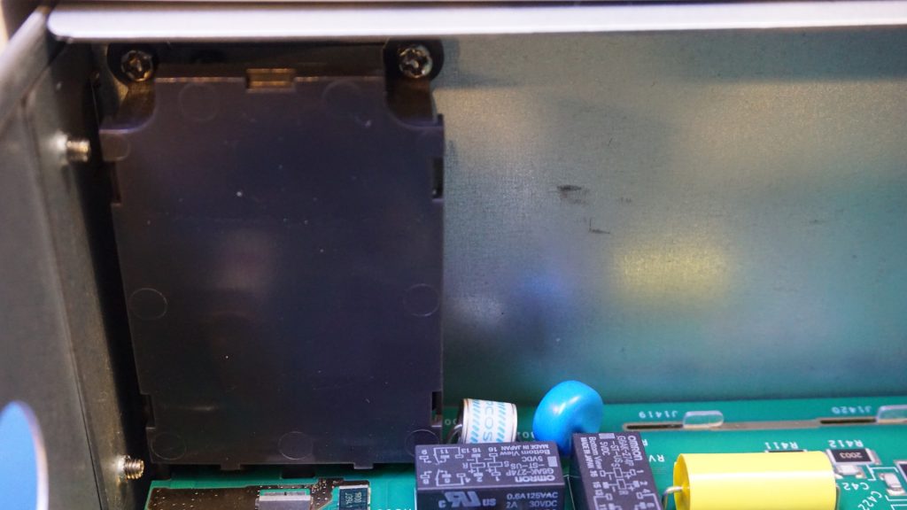
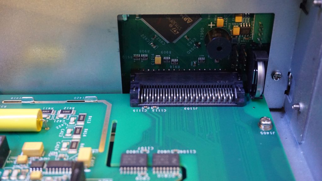
Here is a picture main PCB.
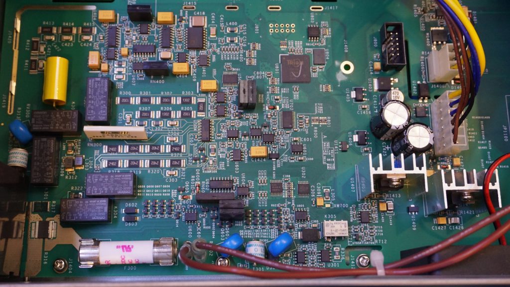
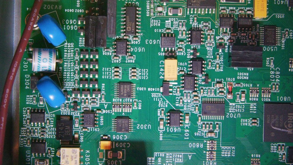
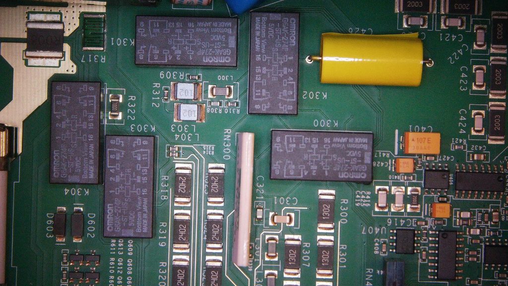
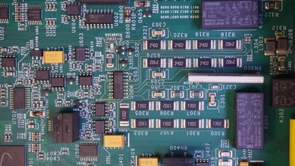
And here are a couple of closeup pictures. You can see the protection MOVs and gas discharge tube in the picture to the left below and the relays in the picture to the right below.
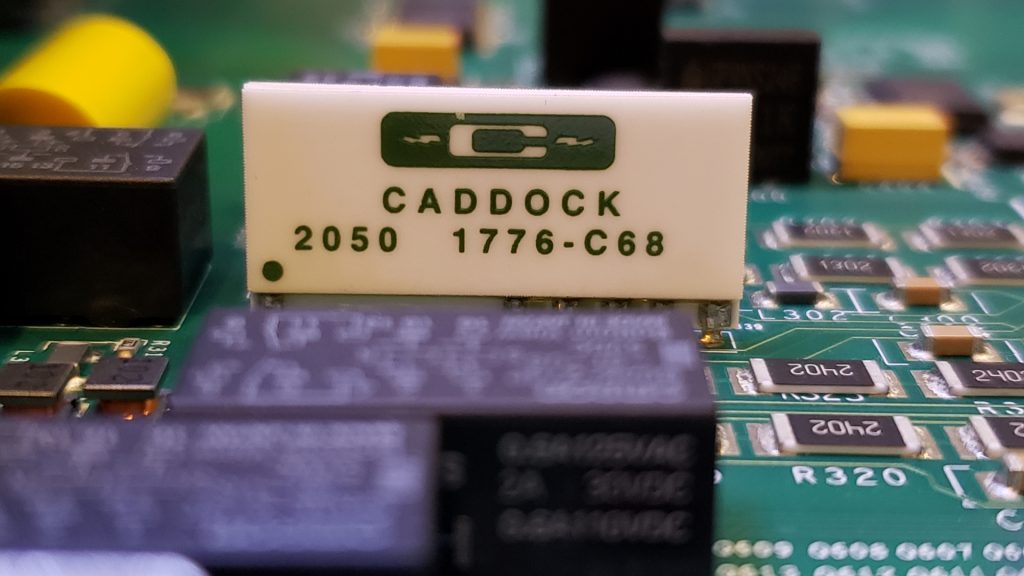
Here is a closeup picture of the Caddock 1776-C68 voltage divider resistor network used in the meter.
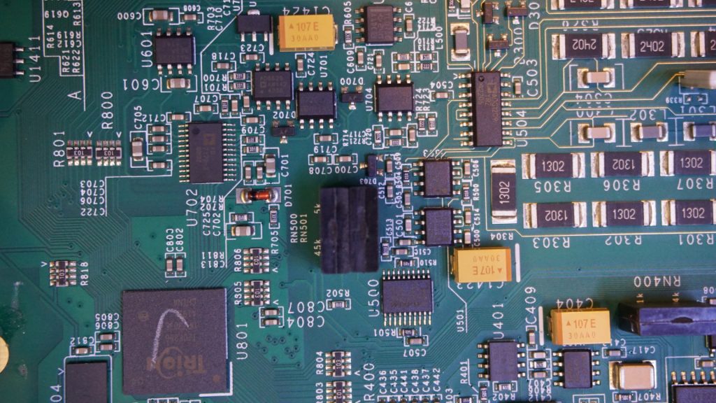
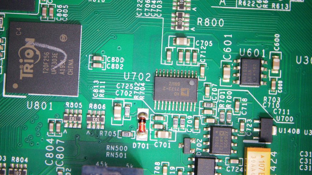
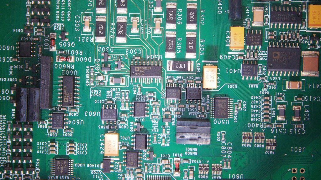
In pictures below you can see the main FPGA used is a Trion T20F256C4. The main ADC used is an Analog Devices AD7172-2, a 24-bit sigma-delta ADC which is capable of up to 31.25 kSPS sampling rate. This fast sampling rate attributes to the fast display update rate of the meter. In these images, you can also spot the voltage reference used, namely the MAX6225. Some of the Opamps used in this meter are AD8629‘s.
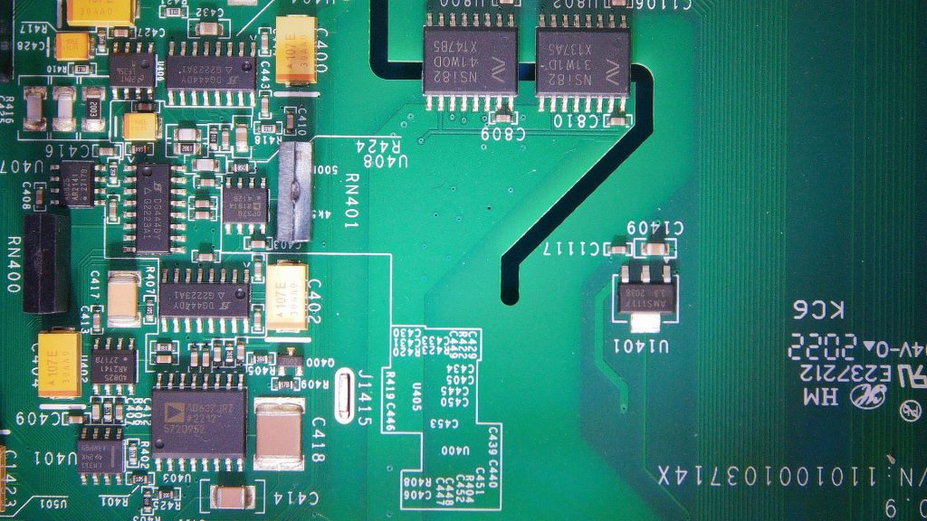
The true RMS converter used is an AD637. In the picture to the right below you can see the PCB revision.
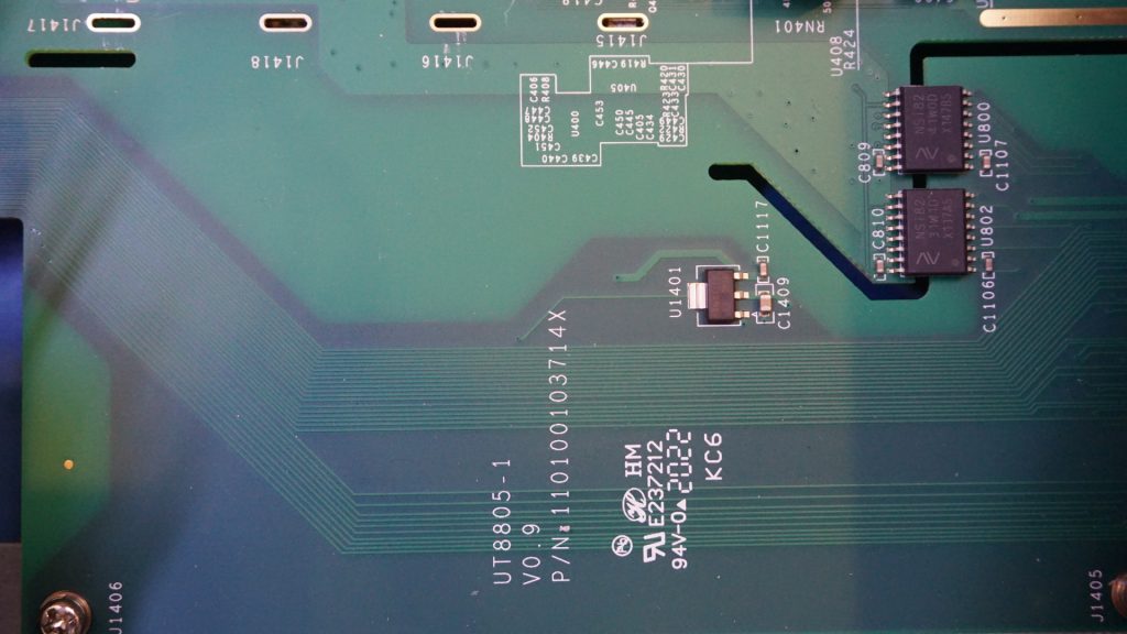
And finally, in the picture below, you can see the guard traces which is used to prevent leakage from the high impedance traces.
Here is the teardown video:

