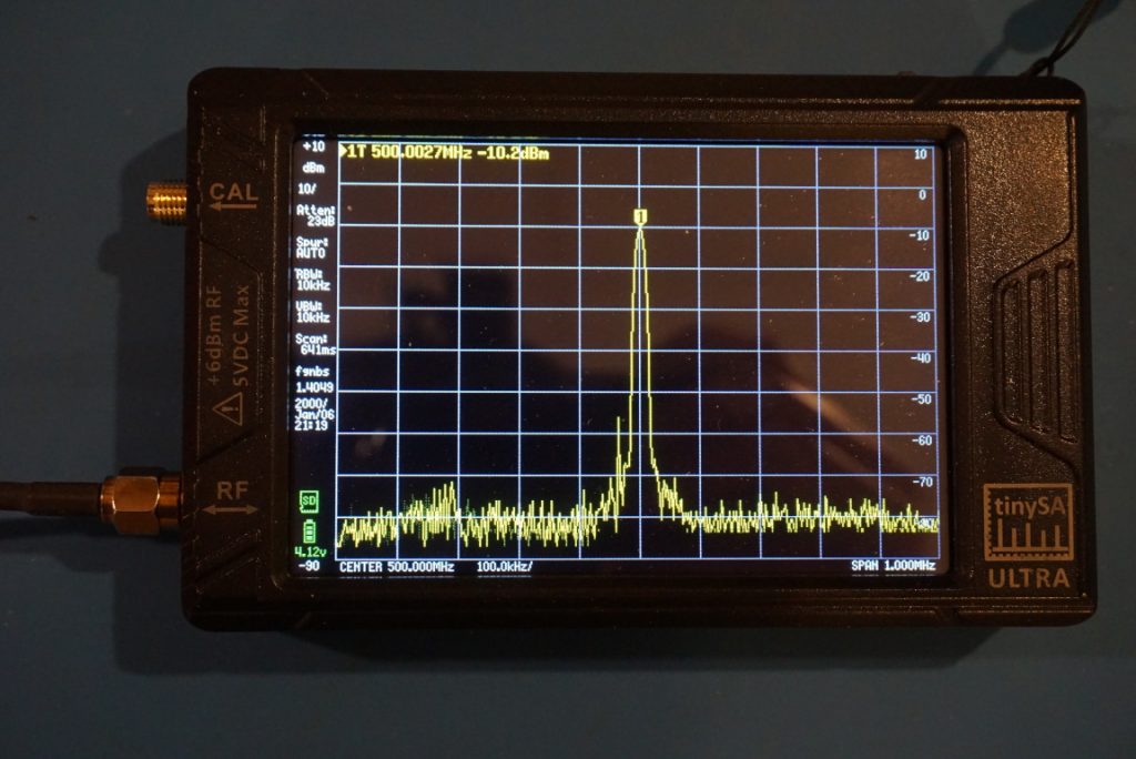
tinySA Ultra is an affordable spectrum analyzer geared towards HAM radio operators, RF enthusiasts and electronic hobbyists. With the Ultra mode enabled, it boasts a calibrated frequency range up to 6 GHz and can observe signals up to 12 GHz. Besides the spectrum analyzer capability, it also has a built-in RF synthesizer that can output frequencies up to 5.4 GHz with the ability to apply AM/FM modulation and do sweep.
I did a detailed review of the tinySA Ultra and compared the captured spectrum with my HP8566B as a reference. You can check out the review below:
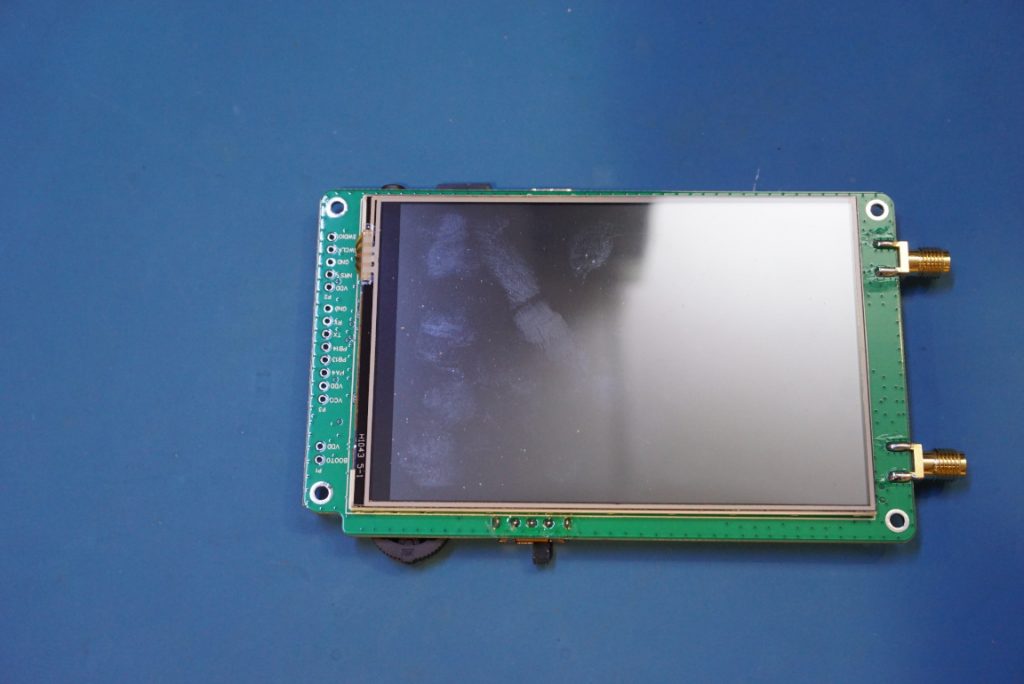
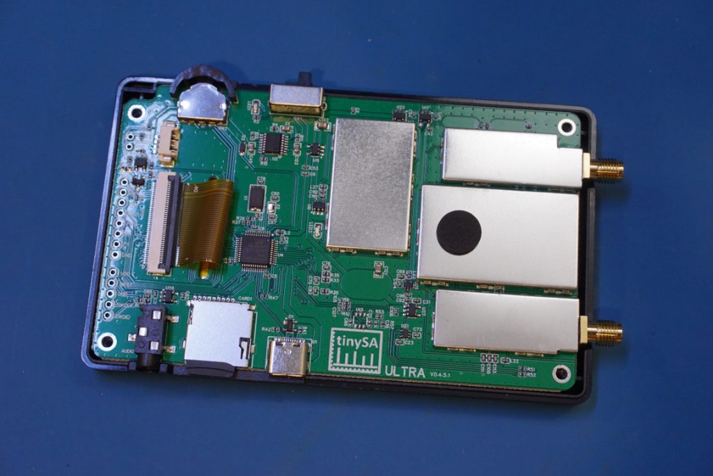
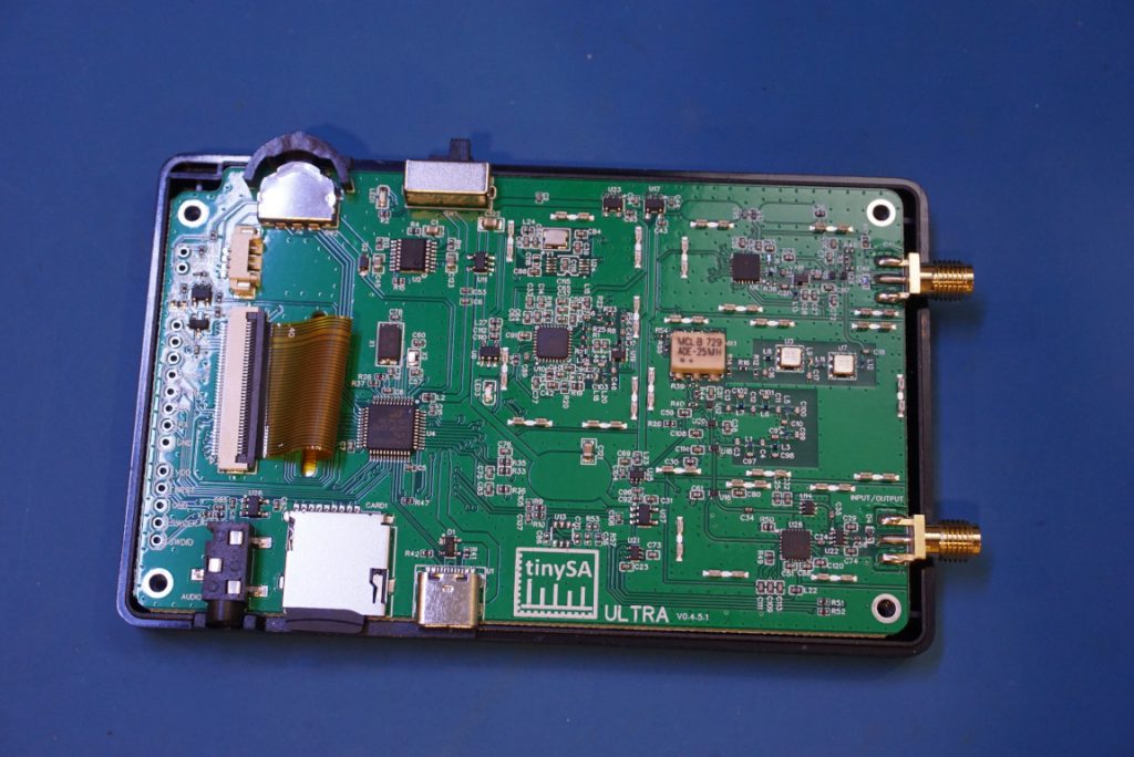
In this blog post, let’s take a look at some of the teardown pictures.
tinySA uses a single PCB design. Thanks to the clip-on shielding cans, I was able to remove them and reveal the circuitry underneath.
tinySA uses the standard heterodyne swept spectrum analyzer technique. Input signal is mixed with the LO and then the down converted signal is further processed by the onboard processor.
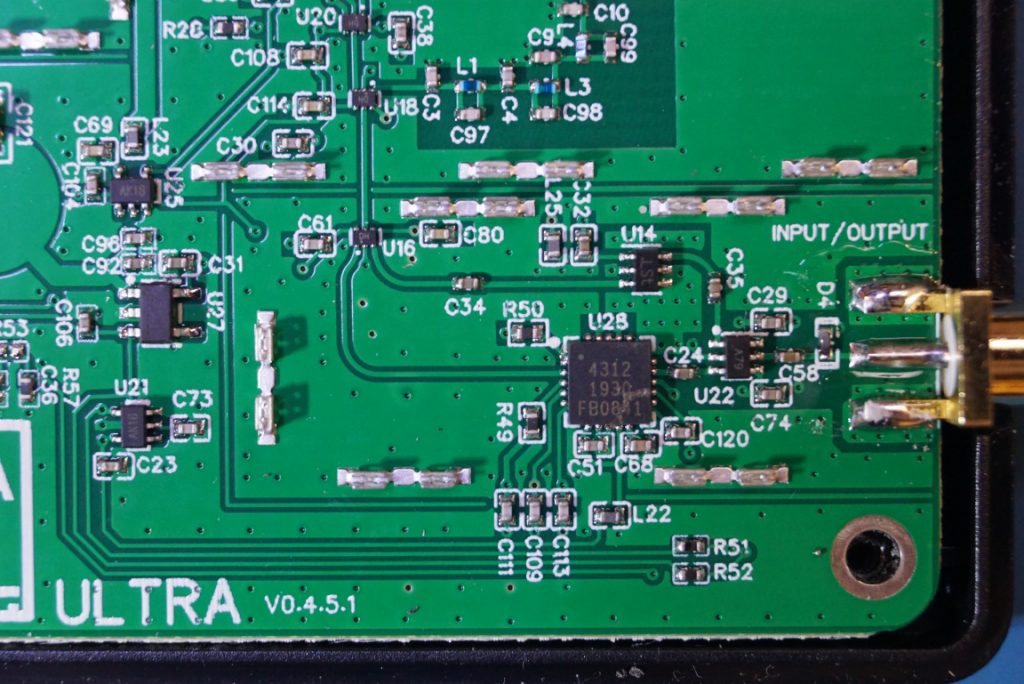
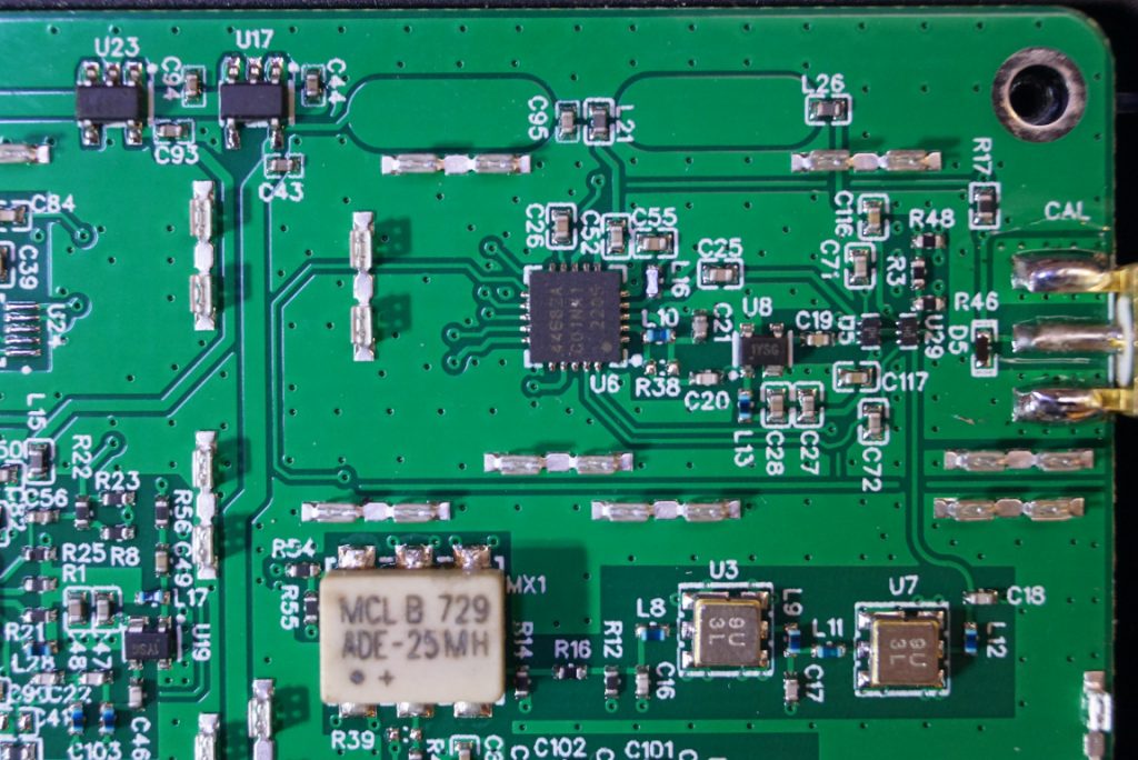
The image to the left below corresponds to the RF input and output section. The chip marked 4312 is a PE4312 6-bit RF digital step attenuator chip. U14 is the LNA, which is a BGA2817 monolithic microwave integrated circuit (MMIC) wideband amplifier. And the chip marked U22 is an input switch (XA17-G4K) with a working frequency range between 20MHz and 4 GHz. The image to the right corresponds to the calibration output section. The QFN chip is an Si4468 transceiver chip.
The larger component marked ADE-25MH is is a frequency mixer that is capable of mixing signals between 5 MHz and 2.5 GHz.
The synthesizer chip used in the tinySA ultra is an Analog Devices ADF4350A, which has an output frequency range up to 4.4 GHz. The chip above the power switch marked as U2 is a CS5181E charging controller.
The microprocessor used is an STM32F302, an ARM based Cortex M4 processor.
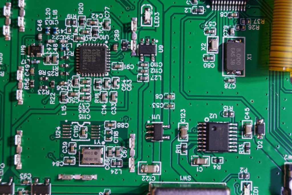
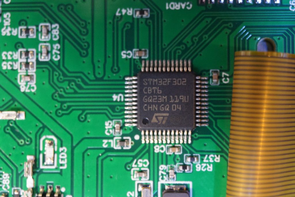
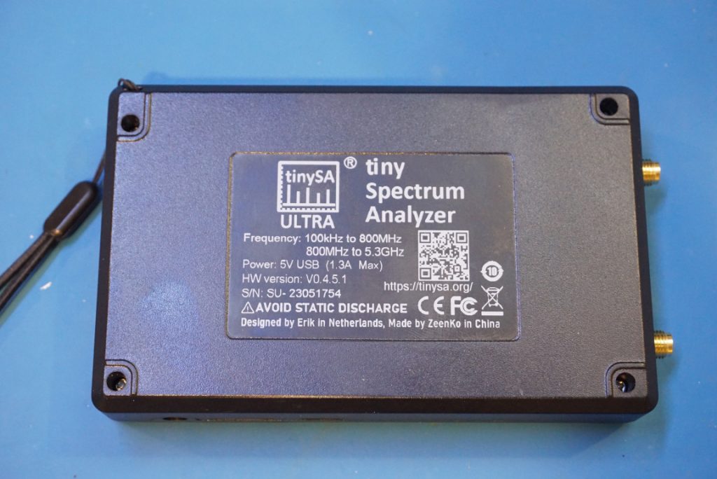
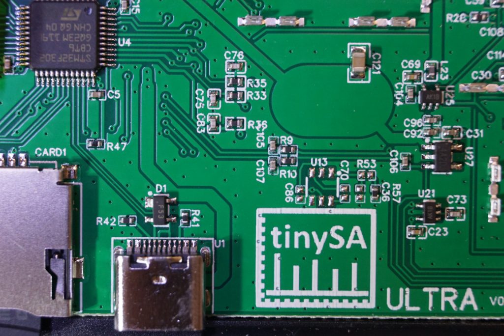
According to the silkscreen, the board version is V0.4.5.1. In the picture to the right below, you can see the programming headers.
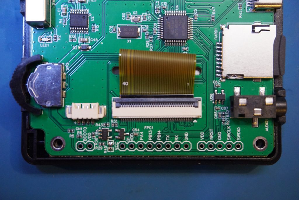
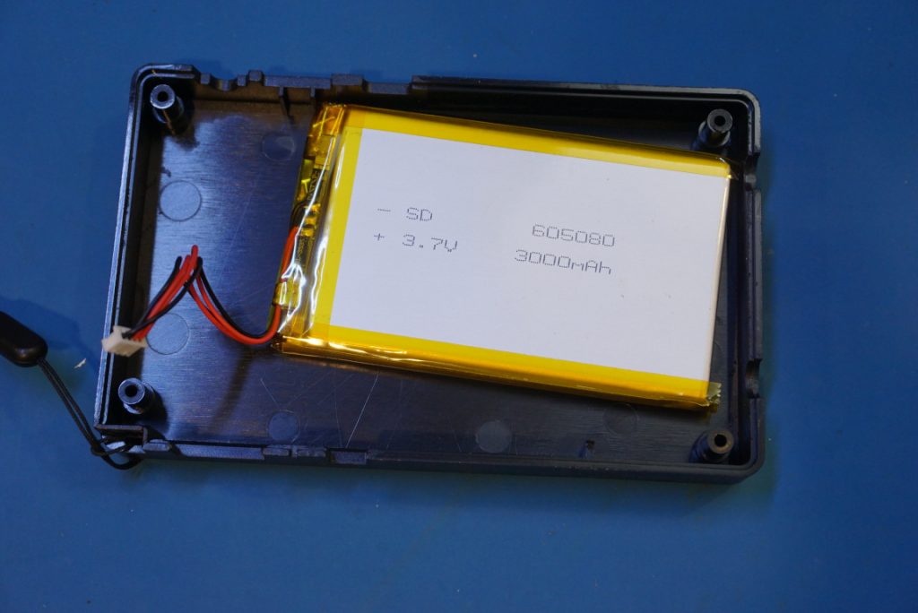
tinySA Ultra is powered by a 3 Ah Li-Po battery.
