I received yet another NanoVNA for review. This time it is a S-A-A-2 (NanoVNA V2) with N connectors instead of SMA connectors found on the other NanoVNAs I reviewed before. This NanoVNA is based on a fully open-sourced design, with schematics readily available. Compared to the NanoVNA-F V2 I reviewed a while back, the specifications are very similar. This VNA is capable of sweeping between 50 kHz and 3 GHz. The LiteVNA I reviewed last time has broader frequency range and is capable of scanning up to 6.3 GHz.
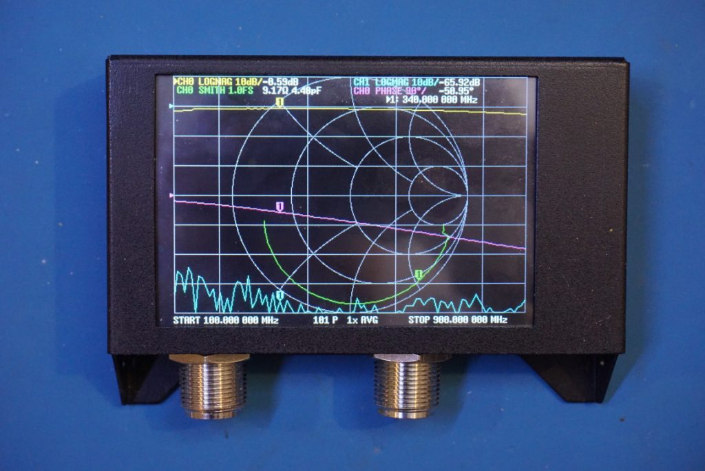
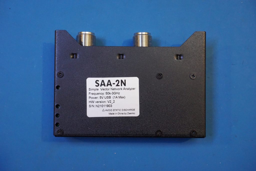
Unlike the other NanoVNAs we had done teardown with, the SAA-2 utilizes a two-board design with two PCBs stacked together.
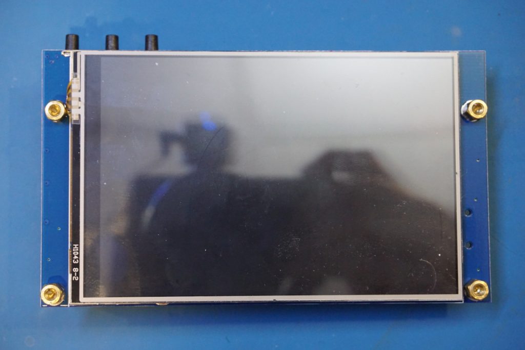
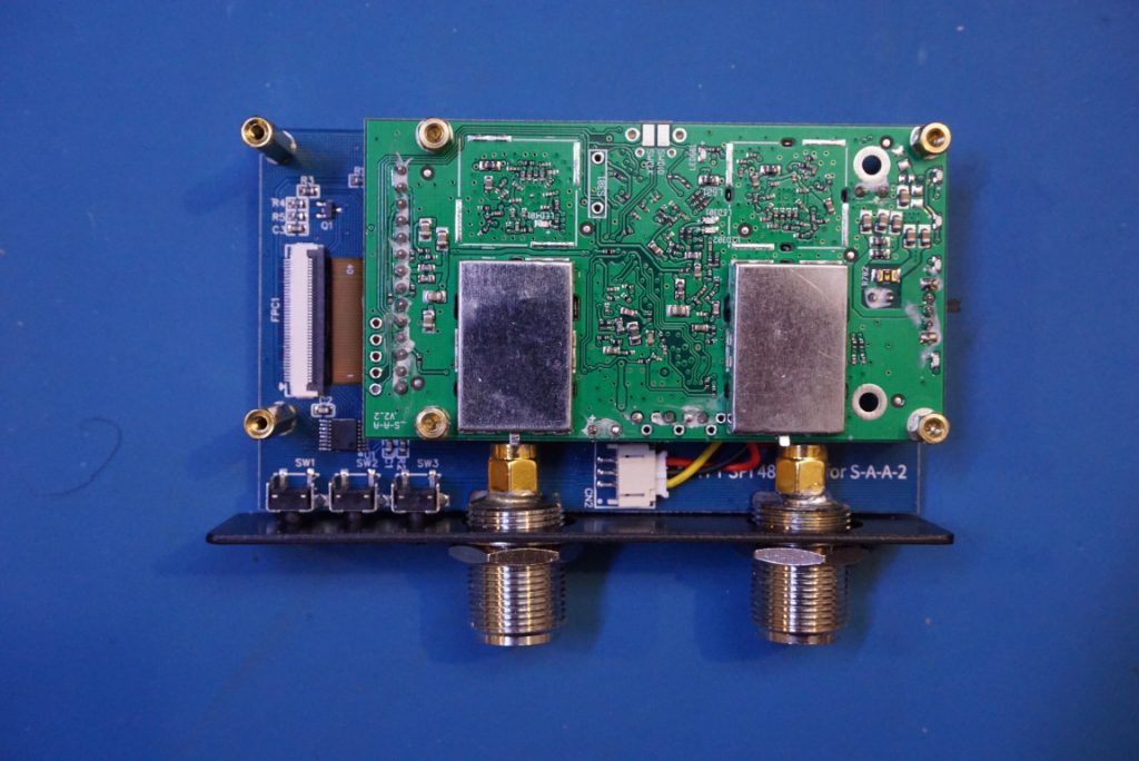
Here we have the two stacked boards dissembled. The pictures below are the back side of the LCD boards. The battery used is a 3Ah LiPo battery, which is plenty as the current consumption is at 400mA maximum. This battery capacity should give you a runtime of at least 7 to 8 hours. In the picture to the right below, you can see the touch screen controller HR2046.
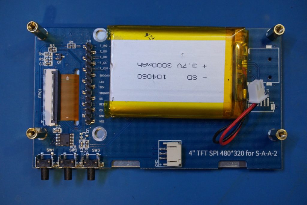
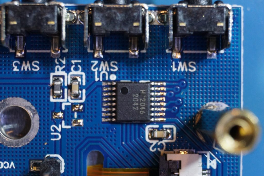
Below is a picture of the back side of the main board with the shielding cans removed.
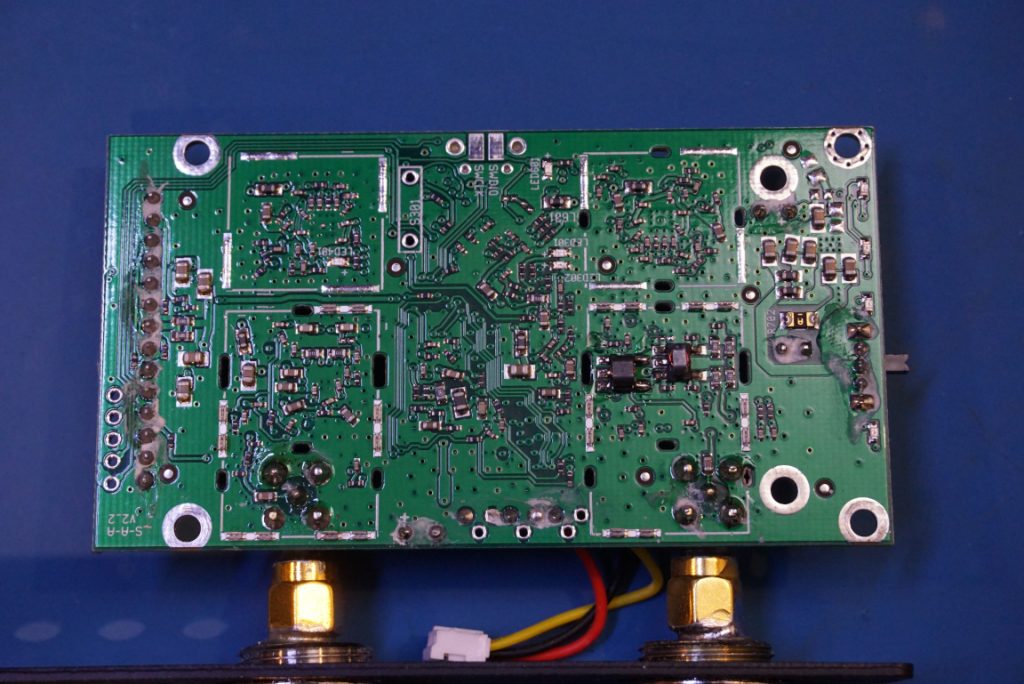
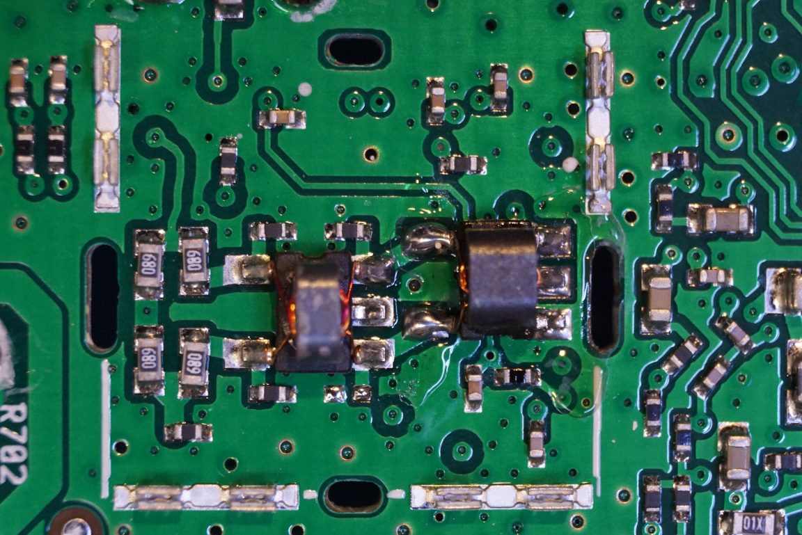
The picture to the left below is what’s under the cover of the S11 port input section. The two RF transformers form part of the directional coupler circuitry. The picture to the right below shows the passives near the S21 port.
The pictures below are for the component side of the main PCB. Interestingly, although the footprints call for four shielding cans, only two are actually in place.
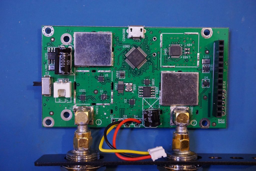
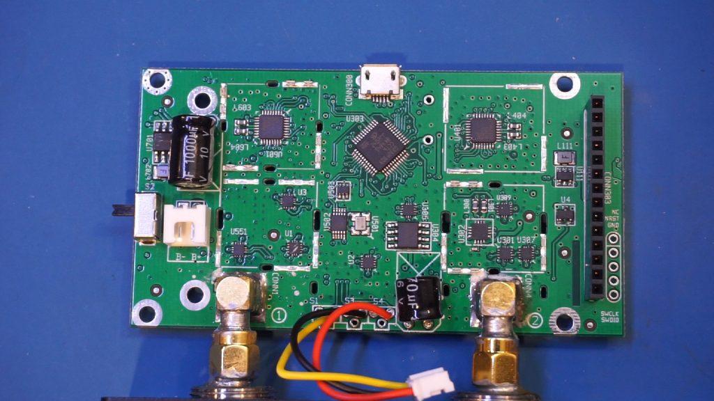
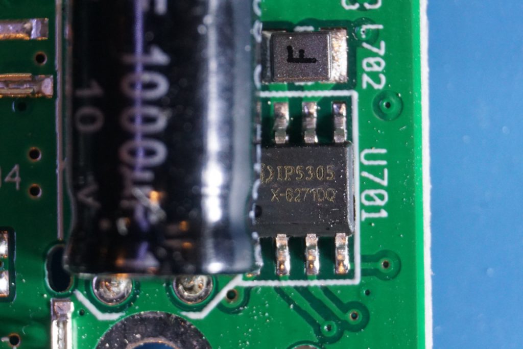
To the far left of the circuit board you can see an IP5305 charging controller which is responsible for charging the onboard LiPo battery.
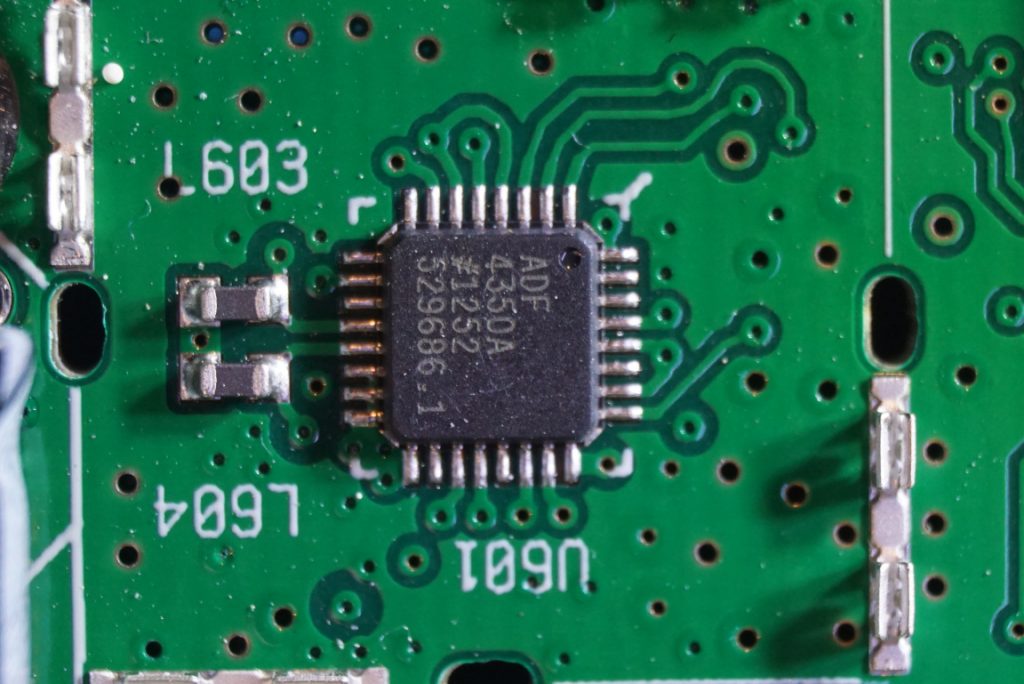
The SAA-2 architecture utilizes three synthesizers and VCOs for both LO and stimulus signals. Two ADF4350‘s are used. One for the transmitter section and one for the receiver section. The ADF4350’s are responsible for sweeping between 140 MHz to 3 GHz.
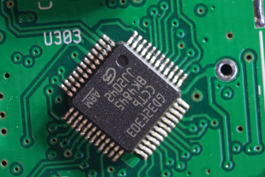
The microcontroller used is a GD32F303, which is a 32bit ARM Coretex M4 MCU.
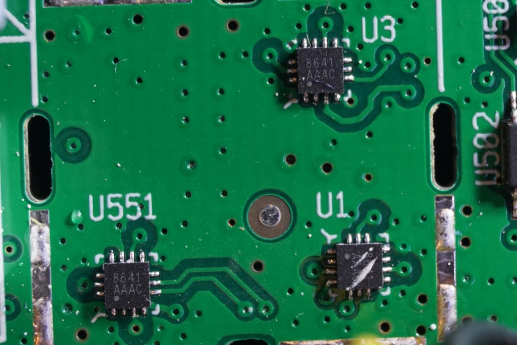
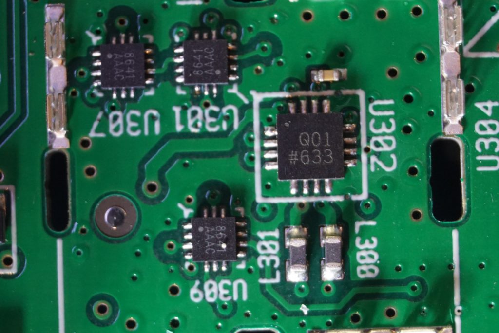
Given the switched receiver architecture design, many 8641‘s are used for switching the RF signal paths connected to the mixer.
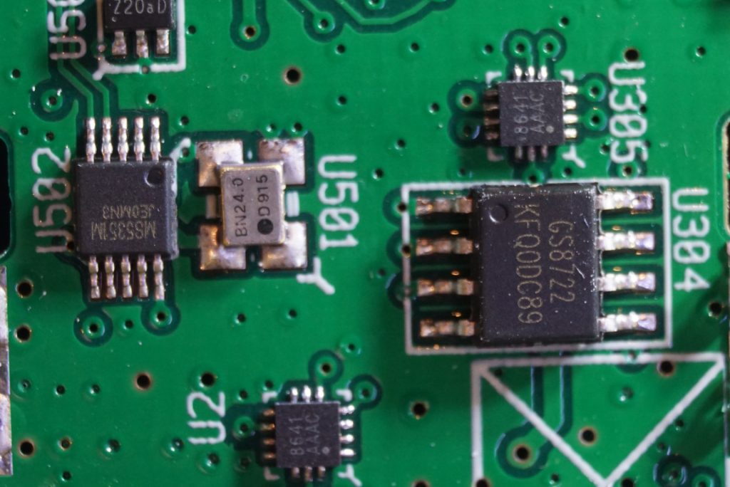
The picture below shows a close-up of the base-band amplifier portion of the circuitry. Here a GS8722 rail-to-rail Opamps IC is used for the base-band signal amplification. Note the MS5351 I2C COMOS clock generator chip below, this chip is the third synthesizer for frequencies below 140 MHz and is shared between the transmitter and receiver channels.
The picture below shows the mixer portion of the circuitry. The IC marked as Q01 below is an AD8342 which is an active mixer.
Here is a detailed teardown video of the SAA2 NanoVNA:

