Semiconductor curve tracers were frequently used in analog circuit designs many decades ago, at a time when discrete semiconductor devices were in dominance and ICs were scarce. While curve tracers are no longer widely used nowadays due to the ubiquity of digital circuitry and computer aided designs, they are still quite popular in the educational world and among hobbyists. In this and the next post, I will discuss some of the design considerations of a curve tracer that I built and show some real-world measurement results.
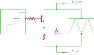
A typical use of a curve tracer is to generate the V-I characteristics of the device under test (DUT). The following diagram illustrate how a typical configuration works when the DUT is a BJT.

In the figure above, a staircase waveform is fed into the base of a NPN transistor via a base resistor R2. For each step in the waveform, a different base current (Ib) is generated. When the input waveform voltage is sufficiently large, the voltage drop between the base and emitter junction (Vbe) can be ignored and thus:
\[I_b\approx\frac{V_{bi}}{R_2}\]
where Vbi is the voltage of the ith staircase. This arrangement is usually good enough for most cases and this is what I used in my design as well. If we need more accurate characterizations of different Ib’s, we can either use a variable current source (which increases the circuit complexity) in place of the staircase waveform generator or simply use the same design but add a current sensing OpAmp to read back the actual base current.
A sweep voltage is applied between the collector and the emitter. The sweep waveform is usually a symmetrical triangular wave so that characteristic curves for both sweep directions can be captured. When we only care about the characteristics in one direction (say when the voltage is ramping up) we could use a sawtooth waveform instead. The linearly of this swept waveform is not significantly important, and in many curve tracer implementations (like this one) the sweep waveform is simply bridge-rectified from the transformer directly. Since the rectified AC signal is sinusoidal, the end of the curve tends to be brighter than the rest of the curve compared to that using a triangular swept signal.
In the diagram above, the collector current is measured at the emitter side via the voltage drop across the emitter resistor. While technically speaking, the measured voltage corresponds to Ie not Ic, but usually Ib is small enough and can be safely ignored without any significant impact to the overall measurement accuracy. For some power devices however, the common emitter gain (hfe) can be quite small (e.g. in the teens) and the collector current measurement can be off by quite a bit when the measurement is done on the emitter side.
The main reason we prefer the emitter side Ic measurement is because it is very easy to implement. When we use this implementation, we could use the emitter as a virtual ground and measure both Vce and the voltage drop across R1 using the two channels of an oscilloscope easily. Of course if your intention is to get the most accurate measurement in all circumstances at all cost, you could move the resistor to the collector side and use a differential amplifier to measure the current flowing through instead. There is another hurdle to the collector side current measurement implementation. Since the DUT can be either N-type or P-type, it will require the differential amplifier to have a common-mode input range that includes both rails. Bi-directional current-sensing OpAmps that have this characteristics tend to be very expensive.
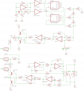
After we covered the basics, let us take a look at my design below:

Staircase Waveform Generator
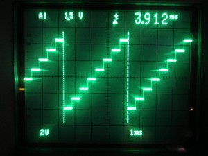
IC4A (1/6 74HC04) along with the watch crystal (32768 Hz), R1, R2, C1 and C2 form a simple oscillator which generates a 32.768 kHz clock signal. The clock signal is then buffered by two inverters in parallel (IC4B and IC4C). The buffered square wave feeds into the clock of a dual 4-bit ripple counter 74HC393. I used one of the two counters (IC5B) to down-sample the clock to 2048 Hz (32768/16), and then use the three bits of the other counter (IC5A) to drive a R-2R ladder to generate the stair waveform. Note that QD is connected to CLR in IC5A, so the counter only counts to 8 instead of 16. So we have 8 discrete staircases. The staircase signal has a frequency of 256 Hz (2048/8).
Because we used TTL logic, the resulting staircase waveform is between 0V and 5V. In order to drive either N-type or P-type devices, we need the output to be either above 0V or below 0V as well. How do we achieve this?
IC2B solves the problem. When pin 5 is grounded, IC2B becomes an inverting amplifier. The gain is set by -R11/R9=-1. When pin 5 is floated, IC2B becomes a non-inverting amplifier with a gain of 1+R11/Rg. Since pin 5 is float, Rg=∞ and the gain of the non-inverting amplifier is unity. IC2A also forms an inverting amplifier but with a gain of 2, so the overall output signal is either between 0 to 10V or 0 to -10V depending on the polarity selected. Finally the output from IC2A is used to drive a simple push-pull stage so that we can draw more current from the circuit than the OpAmp alone could provide. Note that the feedback loop of the output OpAmp (IC2A) is connected to the collectors of the push-pull stage and not the output pin (pin 1), this is important as the OpAmp will be able to compensate the Vbe drop in the push-pull stage and thus avoiding signal distortion.
Here is a picture showing the output staircase waveform:

Triangular Waveform Generator
The staircase waveform generator mentioned above is used to generate the discrete Ib’s in the V-I plot. Now let us take a look at the generation of the Vce sweep signal.
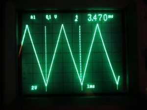
IC1A and IC1B form a triangular waveform generator. In this configuration, IC1A is configured as a threshold detector with hysteresis, and IC2B integrates the threshold detector output (either Vcc or Vdd) and outputs a triangular wave. Please see TI’s AN-20 for more details. The generated triangular waveform has a peak-to-peak voltage of roughly 2V and is bi-polar. In order to generate either a positive (for N-type DUT) or a negative (for P-type DUT) ramp signal, an “adder” circuit is used. The adder is built around IC3B, which is an inverting amplifier. It amplifies the in-coming signal roughly by three. The input to the inverting input of IC3B is the sum of the input triangular signal and a fixed potential reference defined by the wiper positions of either R20 or R21. By adjusting these two trimmers, we can shift the output waveform to either all positive or all negative and thus obtaining a suitable sweep signal for either N-type or P-type devices.
Finally, IC3B’s output is amplified by the times two inverting amplifier formed by IC3A and its output is again buffered via a push-full configuration. The final output of the triangular waveform is shown below:

The vertical sweep frequency does not need to be in sync with the staircase waveform. In my case, these two frequencies happened to be pretty close. In general, you want both waveform generators to operate in the hundreds Hertz range. Too low of a sweep frequency makes the display flicker and too high of a sweep frequency would require higher bandwidth and slew rate OpAmps in order to avoid waveform distortion.
Other Considerations
As mentioned earlier, my design philosophy was to keep everything simple and yet make the curve tracer fully functional. So some of the aforementioned sacrifices were deliberate design choices to make keep the curve tracer as simple as possible.
One thing you could easily improve upon this design is to use better spec’d OpAmps. I used LM258/LM358 because that’s the OpAmp I happen to have on hand. They definitely get the job done, but there are some limitations that you should be aware of.
First is that these general purpose OpAmps have a rather low bandwidth (<1MHz unity gain bandwidth) and very low slew rate (<0.3V/us), this means that you can not make either waveform faster than a couple hundred Hertz without noticing significant degradation. Second, due to the small slew rate, there is some artifacts introduced in the triangular sweep signal waveform (some tiny spikes near the vertices of the triangular waveform). This artifact is caused by the slow switching of the comparator when the polarity of the signal changes. One way to alleviate this issue is to keep the waveform frequency lower by increasing R16 and the output amplitude lower by increasing R15. And last but not least, the OpAmp is not rail-to-rail, which means the maximum sweep voltage would always be at least 1V below the supply rails. LM258/LM358 can operate up to ±15V, which is usually good enough for most parameter tracing activities. But if you intend to observe the breakdown behaviors of the DUT's, you will need to use OpAmps that can operate under higher supply voltages. One such OpAmp comes to mind is TI's OPA452/OPA453, which is capable of operating up to ±40V supply voltage.
In my next post, I will show you some test results from the curve tracer I built. Stay tuned.

