Basic constant current dummy load using an Op Amp and a by-passing MOSFET is very easy to build and had been made quite popular following Dave’s video on EEVBlog. I happened to have an old aluminum hard disk cooler case collecting dust. The die-cast aluminum case is relatively thick, making it an excellent heat sink. So I thought why not use it to build a dummy load myself?
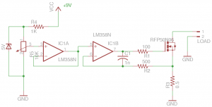
The circuit I am using is pretty standard, although it has been modified a little bit from what you saw in Dave’s video and I will explain a little bit here.
The Op Amp I used is a general purpose LM358N. A simple Zener diode is used to generate a voltage reference at around 5V. This reference voltage is then buffered by IC1A to provide the voltage reference to the Op Amp that drives the by-passing MOSFET. The reference voltage range along with the current-sensing resistor value (R3) determine the current sink capability. In my case, the desired maximum current of this load is 10A. So I chose 5V as the voltage reference with a 0.5 Ohm current sensing resistor. A benefit of using 5V is that this circuit can be easily controlled from an MCU. But for now, the current is controlled by a 10K multi-turn trimpot.
The buffered voltage reference is then passed into the current sink formed by the second Op Amp and the MOSFET. The feedback loop of the Op Amp ensures that the voltage drop across the current sensing resistor is the same as the reference voltage coming from IC1A. R1, R2 and C1 form a compensation network to ensure stability.
The choice of the by-passing MOSFET largely depends on the output current requirements and the Vgs-Ids characteristics. While you typically want to use a logic-level MOSFET if the gate needs to be controlled from an MCU output, using a logic-level MOSFET is not strictly necessary. It all depends on what is the pass-through current requirement at the maximum attainable gate voltage (in this case, it is 5V). The MOSFET I used is Fairchild’s RFP50N06. Even though it is not a logic-level MOSFET, it can deliver more than 20 amps saturation current at a Vgs of 5V which is much more than our designed maximum current (10A).

If we take the maximum allowed power dissipation of RFP50N06 into consideration, we will find that Vds is limited to roughly 12V at the highest load current. In reality though, the maximum Vds allowed for a single MOSFET is likely to be much lower than 12V. So in my design, two RFP50N06 are paralleled (not shown in schematics) so that the maximum allowed power dissipation can be increased.
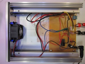
The following picture shows the above mentioned circuit built on a protoboard. The board mounts nicely inside the hard drive cooler aluminum case. The MOSFETs are mounted on the sides of the interior case walls using the existing mounting holes. The original hard drive cooler has a cooling fan mounted towards the front, which provides some airflow to help cooling down when under load.

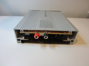
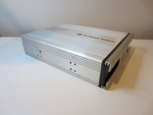
Here is what this constant current load looks like when everything is assembled together.
 |
 |
Because LM358N is not a rail-to-rail operational amplifier, the load current will not go all the way down to 0 when the input voltage is set to zero. Depending on the characteristics of the MOSFET, this current could range from a few milli-amps up to 100 mA. For RFP50N06, the minimum load current is measured at around 50 mA which should be small enough for most uses. If much lower minimum current is required, a better spec’d and preferably a rail-to-rail Op Amp can be used. Another thing to keep in mind is that the input bias current of the Op Amp affects the linearity of the current-setting, but this should only be of a concern if the circuit is used as a low current (e.g. in the micro-Amp range) load. In that case, you will need to pick an Op Amp with a much lower input bias current.

