I picked up an AD9850 DDS module on eBay an couple of weeks ago and decided to build a MCU controlled DDS function generator with it to replace my crude frequency generator I built earlier.
These AD9850 modules are sold very cheaply on eBay. Some people had questioned whether counterfeit or QA-rejected chips were used in these modules. While it is highly likely that these modules — sold at below the cost of the chip — do not meet the all the specifications in the datasheet, they actually work pretty well. The module I received works all the way up to the maximum specified frequency (CLK/2 62.5 Mhz). The amplitude of the output waveform is greatly attenuated after around 30 Mhz however, but this is most likely due to the low pass filter used rather then the limitation of the chip itself. The PCB layout of these boards are not particularly well suited for high frequency operations either. But for hobby uses, the achievable frequency range and the waveform quality should be more than adequate.
The schematics of the module can be found in many places on the web. This one I found appeared to be very accurate. Controlling the AD9850 with an MCU is also rather straight forward. The easiest way is to use the serial interface AD9850 provides to serially shift the turning words into the chip for frequency adjustment. I used an Arduino (ATmega328P) to interface the module. As you can see in the code snippet for the AD9850 below, only four pins are needed to control AD9850 via serial updates.
int PIN_RESET = 13;
int PIN_FREQ_UPDATE = 12;
int PIN_CLOCK = 11;
int PIN_DATA = 10;

void AD9850Reset() {
    digitalWrite(PIN_FREQ_UPDATE, 0);

    digitalWrite(PIN_RESET, 0);
    digitalWrite(PIN_RESET, 1);
    digitalWrite(PIN_RESET, 0);

    digitalWrite(PIN_CLOCK, HIGH);
    digitalWrite(PIN_CLOCK, LOW);

    digitalWrite(PIN_FREQ_UPDATE, 1);
    digitalWrite(PIN_FREQ_UPDATE, 0);
}

//frequency in Hertz
void AD9850Update(double frequency) {
    unsigned char i, w;
    long int tuningWord;

    tuningWord = frequency* 4294.967296f / 125.0f;

    shiftOut(PIN_DATA, PIN_CLOCK, LSBFIRST, tuningWord);
    shiftOut(PIN_DATA, PIN_CLOCK, LSBFIRST, tuningWord >> 8);
    shiftOut(PIN_DATA, PIN_CLOCK, LSBFIRST, tuningWord >> 16);
    shiftOut(PIN_DATA, PIN_CLOCK, LSBFIRST, tuningWord >> 24);
    shiftOut(PIN_DATA, PIN_CLOCK, LSBFIRST, 0x0);

    digitalWrite(PIN_FREQ_UPDATE, 1);
    digitalWrite(PIN_FREQ_UPDATE, 0);
}
Function AD9850Reset resets the address pointer to W0. Typically you only need to call AD9850Reset once upon power up, during the initial MCU configuration phase.
Function AD9850Update updates the chip output to the frequency value passed in (in Hertz). The five control bytes (32-bit turning words plus 8-bit for control and phase) are serially shifted into AD9850 via shiftOut. Since we don’t need to worry about the phase of the generated signal, the last byte is hard-coded to 0.
The full code listing for the DDS function generator can be downloaded towards the end.
AD9850 has a frequency resolution of 0.0291 Hz (with 125 MHz reference clock), so mHz resolution can be achieved.
Control Interface Design
To make the final DDS function generator more useful, here are some of the features I had in mind:
- Frequency inputs are done using numeric keypad
- Able to save/recall frequency settings
- Adjustable pulse width for the PWM output
- Able to enter/display frequencies in mHz/Hz/MHz
Based on the above requirements, I built a prototype on breadboard to test out the functionalities.
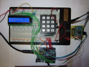
As a bare minimum, 17 control pins are needed from the MCU (4 for AD9850, 7 for the 3×4 keypad and 6 for the 2×16 LCD). This leaves only one spare pin (technically speaking, the Rx/Tx pins used for serial communications can also be utilized, but then I would need to use an external programmer to program the chip) on the ATMega328P. Of course, if you use serial protocol keypad and LCD you will have plenty of unused pins left. For the spare pin, I decided to add a tactile switch which serves as the “function” button.
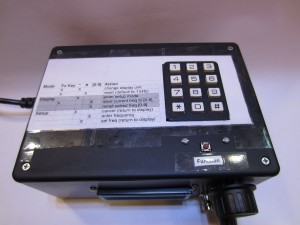
The following table shows how each of the desired function is achieved using the function button in conjunction with the keypad. The “X” in the table means that a key with the corresponding column header is pressed. For instance if the LCD is currently in display mode, pressing the function key and a number on the numeric keypad will recall the frequency setting that was previously stored in that memory slot.
| Mode | Fn | * | # | [0-9] | Action |
| Display | X | enter frequency setup screen | |||
| X | X | change to the next display unit | |||
| X | X | reset output frequency to default (1 kHz) | |||
| X | X | save the current frequency to the memory slot indicated by the numeric key | |||
| X | recall the frequency stored in the memory slot indicated by the numeric key | ||||
| Frequency setup | X | Cancel, go back to the display screen with the previously selected frequency | |||
| X | X | change to the next display unit | |||
| X | X | reset output frequency to default (1 kHz) | |||
| X | set the frequency using the numbers/unit entered and return to display mode |
During the initial power up, the DDS function generator’s output frequency is set to 1 kHz in code. To change the output frequency, press “*” first to switch to the frequency enter screen. The frequency units (mHz, kHz, MHz) can be cycled through by holding down the function button while pressing “*”. Because the keypad does not have a decimal key, you will need to switch to milli-Hertz range to enter frequencies with a resolution finer than 1Hz. After you have entered the desired frequency with the keypad, press “#” to set it. The screen will then change back to the normal display mode (as opposed to the frequency enter mode) with the output set to the updated frequency.
Up to 10 different frequencies can be stored in MCU’s EEPROM to allow fast recalls. This is achieved by pressing the function button and a numeric button while in display mode. The current displayed frequency will be stored into the memory slot indicated by the number ([0-9]) along with the unit used.
To recall a stored frequency, simply press the number on the keypad in display mode. If the recalled memory slot is empty, the recall will be ignored. You can take a look at the code included at the end to see how everthing is done.
Final Build
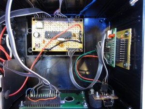
The picture below shows the layout of the circuitry inside the project box. To ensure that the output signal is as clean as possible, both the power supply portion and the AD9850 portion are shielded (the shield on the AD9850 side was removed for the picture), and both the outputs (square wave output via square wave 1 pin and the filtered sine output via sine 2 pin) are connected to BNC jacks with short wires. In order to change the duty cycle of the output PWM signal, I desoldered the 10K potentiometer on the AD9850 module and replaced it with a panel mount one.
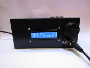
Here are a couple of pictures showing the finished DDS function generator.
 |
 |
And the followings are some oscilloscope captures of the output waveforms:
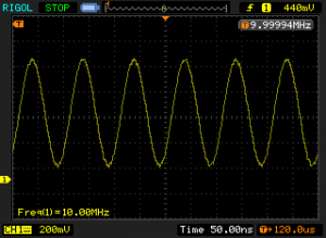
The amplitude of the sinusoidal output starts to drop off as the frequency goes above 30 MHz, which is approximately the cutoff frequency of LC filter used in the circuit. Depending on how this signal is used, you may need to add an additional amplification stage.
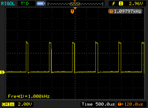
Here are a couple of waveforms from the PWM output (approximately 10% and 90% duty cycle at 1 kHz).
 |
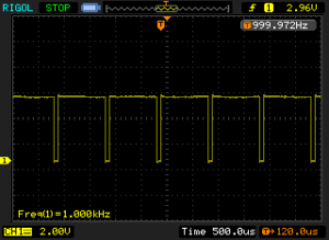 |
The pulse width can be adjusted with the potentiometer. Since the amplitude of the sine signal changes at higher frequencies, the output duty cycle of the PWM signal will also change as a result. So in order to maintain the same duty cycle, the potentiometer may need to be adjusted with different frequency settings.
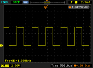
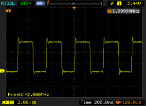
As you can see from below, the square wave output remains pretty clean for frequencies up to a couple of megahertz and after which the overshoots become more pronounced. Better layout could alleviate the problem somewhat. But for general uses, this waveform quality should be sufficient at even higher frequencies.
 |
 |
Download
DDS function generator source code: DDSGen.tar.gz

