I finally got some time to play with the STM32F4-Discovery board I received last year. As for any microcontrollers, learning how to manipulate GPIO pins is always a good place to get started.
Because the STM32F4-Discovery board breaks out most of the pins, it utilizes dual-row headers on each side. This arrangement makes it difficult to use it on a standard breadboard as the adjacent rows would be shorted out. Also, due to some routing constraints, the port pins are not all conveniently located in a sequential manner, which also makes prototyping more difficult.
So the first thing I decided to do was to build an adapter board for the STM32F4-Discovery to breakout all the port pins in a convenient-to-access layout. The picture below shows the the adapter board I built:
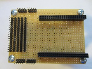
Since there are 80 plus pins to breakout, the wiring is a bit messy on the reverse side as you can imagine. But with some careful planning, the soldering task was actually not that bad. So now I have five rows of header pins, representing PORTA through PORTE. Each row’s layout is as follows:
3.3V Gnd P0 P1 P2 P3 P4 P5 P6 P7 P8 P9 P10 P11 P12 P13 P14 P15 Gnd 5.0V
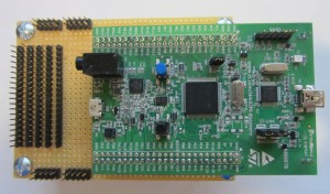
I deliberately chose a 20-pin configuration for each row so that I could use a standard IDE cable (either row) to connect the pins to the breadboard.
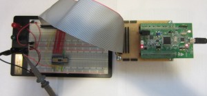
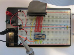
To test my breakout board, I decided to use a parallel DAC as it is fairly easy to work with. In the picture above, I interfaced the STM32F4-Discovery board with an 8-bit parallel ADC AD5330. At a bare minimum, eight data pins and one control pin are needed to control this chip. For simplicity, I configured AD5330 in unbuffered, Vcc referenced mode and set the output gain to unity. More pins will be needed if these parameters need to be controlled programmatically. Since all the five ports on STM32F4 are 16-bit, all the pins can be controlled with the use of just one port.
Here is a picture of the AD5330 portion of the circuit:
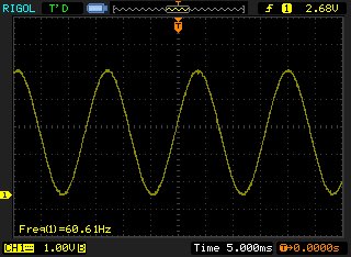
The code below shows how to generate a 60Hz sinusoidal wave with 256 sampling points using the bit-banging method. Given the symmetrical nature of the sinusoidal wave, only data values between 0 and Pi/4 are needed, the values between (Pi/4, 2Pi] are obtained by shifting the values in [0, Pi/4]. The program is compiled and loaded using Attolic TrueSTUDIO.
#include "stm32f4xx.h"

#define PIN_WR GPIO_Pin_8
#define PIN_DATA GPIO_Pin_0 | GPIO_Pin_1 | GPIO_Pin_2 | GPIO_Pin_3 | GPIO_Pin_4 | GPIO_Pin_5 | GPIO_Pin_6 | GPIO_Pin_7

//sine() values between 0 and pi/4
unsigned char ay[]={
		128, 131, 134, 137, 140, 143, 146, 149,
		152, 155, 158, 162, 165, 167, 170, 173,
		176, 179, 182, 185, 188, 190, 193, 196,
		198, 201, 203, 206, 208, 211, 213, 215,
		218, 220, 222, 224, 226, 228, 230, 232,
		234, 235, 237, 238, 240, 241, 243, 244,
		245, 246, 248, 249, 250, 250, 251, 252,
		253, 253, 254, 254, 254, 255, 255, 255
};

void delay(__IO uint32_t n) {
	while(n--);
}

void initAddrAndCtrlPins()
{
	GPIO_InitTypeDef GPIO_InitStruct;

	GPIO_InitStruct.GPIO_Pin = PIN_DATA | PIN_WR;

	GPIO_InitStruct.GPIO_Mode = GPIO_Mode_OUT;
	GPIO_InitStruct.GPIO_Speed = GPIO_Speed_100MHz;
	GPIO_InitStruct.GPIO_OType = GPIO_OType_PP;
	GPIO_InitStruct.GPIO_PuPd = GPIO_PuPd_NOPULL;
	GPIO_Init(GPIOD, &GPIO_InitStruct);
}

void write(unsigned char c)
{
	GPIOD->BSRRH = 0x1ff;
	GPIOD->BSRRL = c;
	GPIOD->BSRRL = PIN_WR;
	GPIOD->BSRRH = PIN_WR;
	delay(280);
}

void initGPIO(){
	RCC_AHB1PeriphClockCmd(RCC_AHB1Periph_GPIOD, ENABLE);
	initAddrAndCtrlPins();
}

int main(void)
{
	initGPIO();

	unsigned char i;

	while (1)
	{
		for (i=0; i<64; i++) write(ay[i]);
		for (i=0; i<64; i++) write(ay[63 - i]);
		for (i=0; i<64; i++) write(255 - ay[i]);
		for (i=0; i<64; i++) write(255 - ay[63 - i]);
	}
}
As you can see, the coding is pretty straightforward. In general, to use any GPIO pins in STM32F4 we first need to enable the clock for that port. Then we set the pins within that port to the desired input/output mode. BSRRH and BSRRL are used to reset and set the pins.
In the write() method, the DAC value is set directly to the lower 8 bits in PORTD. And the WR line is toggled afterwards to set the DAC output. Depending on the speed of the DAC used, some delays maybe required before toggling the WR line to allow the input data to stabilize.
With 256 sample points, the output sine wave is very smooth as can be seen below:
